


CL3/CL1
167
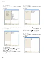
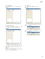
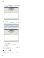
工場出荷時の状態にするためには、
[STORE]
と
[INC]
キーを同時に押しながら電源を立ち上げ強制初期化を実行します。
強制初期化完了後には、
「Flash Memory Initilalizing Finished.」の Confi rmation が表示されるので、
[CLOSE]
を押して通常画
面とし、DANTE のバージョンが出て、右上の ACCESS インジケーターが消えるまで待って終了します。
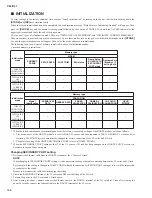
ま た CL に は ユー ザ ー にも 公 開 して い る2 種 類 の 初 期 化 モ ード、
「INITIALIZE ALL MEMORIES」
「INITIALIZE
CURRENT MEMORIES」があるのでサービスなどでは必要に応じて使い分けることも可能。
[STORE]
キーを押しながら電源を立ち上げると表示される特殊モード画面から実行可能。
上記3種類によって初期化される対象のメモリーをまとめると下記の通りになります。
(○が初期化の対象)
初期化の種類
初期化対象メモリー
MRAM
CURRENT
SCENE
SETUP DATA
PORT TRIM
DIO
ステータス
Dante Setup
-CONSOLE ID
-SECONDARY
PORT mode
Dante module
(Brooklyn
II
)
setting data
強制初期化
(工場出荷時)
○
○
○
○
○
○
INITIALIZE
ALL
MEMORIES
○
○
○
̶
̶
̶
INITIALIZE
CURRENT
MEMORIES
○
○
○
̶
̶
̶
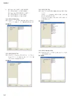
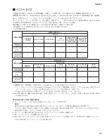
初期化の種類
初期化対象メモリー
FRASH ROM
機種判別
SCENE1-30 0
DATA
LIBRARY DATA
FADER
CALIBRATION
NAME BL
CALIBRATION
CH COLOR
CALIBRATION
USER
BITMAP
強制初期化
(工場出荷時)
̶
○
○
̶
̶
̶
○
INITIALIZE
ALL
MEMORIES
̶
○
○
̶
̶
̶
○
INITIALIZE
CURRENT
MEMORIES
̶
̶
̶
̶
̶
̶
̶
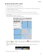
※ 強制初期化(工場出荷時)を実行すると、DANTE モジュールの設定は次のようになります。
1. ダンテモジュールのデバイス名が、BLKN II xxxxxx にリセットされて、再起動後に Y001 ヤマハ CL x-xxxxxx に改名されます。
CL シリーズとI/Oラックを正しく接続をする為にダンテのデバイス名の変更は、不可欠です。
2. Dante の SECONDARY PORT のネットワーク設定は、
「DAISY CHAIN」にリセットされます。
※ DANTE SETUP 画面で SECONDARY PORT 設定や、CL シリーズや I/O ラックの ID を変更した場合は、電源の入れ直
しが必要になります。
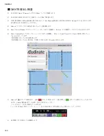
SECONDARY PORT 設定の変更
1. CL シリーズ、I/O ラックの DANTE 端子からイーサネットケーブルを外します。
NOTE
SECONDARY PORT 設定を変更する場合には、CL シリーズと I/O ラックの間の結線方法も変更が必要です。
たとえば、REDUNDANT に設定したときの結線のまま DAISY CHAIN に変更すると、音声のやりとりができなくなります。
設定を変更する前に、まずケーブルを抜いておくようにしてください。
2. CL シリーズの REDUNDANT 設定と I/O ラックのディップスイッチの設定を確認します。
3. CL シリーズと I/O ラックの電源を入れなおします。
4. 約 1 分待ってから、先に I/O ラックの DANTE 端子のイーサネットケーブルを接続してから、20 秒ほど待って最後に CL シリー
ズの DANTE 端子にイーサネットケーブルを接続します。
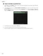
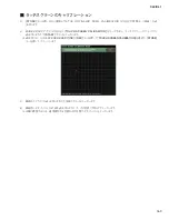
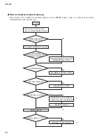
■ イニシャライズ
Summary of Contents for CL3
Page 7: ...7 CL3 CL1 DIMENSIONS CL3 CL1 648 15 201 130 299 667 839 15 201 130 299 667 Unit mm...
Page 95: ...95 CL3 CL1 CPU Circuit Board Pattern side to DSP CN101 2NA WY67750 1...
Page 101: ...101 CL3 CL1 DNTU Circuit Board Pattern side Scale 80 100 2NA WZ20390 5...
Page 102: ...CL3 CL1 102 2NA WY63530 FX Circuit Board WR 63 1 Component side Scale 95 100...
Page 103: ...103 CL3 CL1 2NA WY63530 FX Circuit Board Pattern side Scale 95 100...
Page 105: ...105 CL3 CL1 HAAD Circuit Board Pattern side Scale 90 100 2NA WY64340 2...
Page 107: ...107 CL3 CL1 2NA WY63490 Component side JK Circuit Board WR 63 1...
Page 109: ...109 CL3 CL1 Component side TBPHN Circuit Board WR 06 1 WR 63 1 2NA WY64360 1...
Page 110: ...CL3 CL1 110 Component side PN8 Circuit Board to FD8 CN902 or FD8CN CN902 2NA WY53120 2...
Page 118: ...CL3 CL1 118 Component side PNENL Circuit Board to PN8 CN001 2NA WY53130 1...
Page 160: ...CL3 CL1 160 1 18 LCD Test LCD LCD 1 3 2 9 5 OK NG 1 2 H 3 O X O 4 BOX 5x4...
Page 382: ...7 MBCL CIRCUIT BOARDS A A A A 2NA WY53200 1 MB Circuit Board Component side...
Page 383: ...MBCL 8 MB Circuit Board DSUB PH CONNECTOR ASSEMBLY B B B B 2NA WY53200 1 Pattern side...


![Drolo Stamme[n] Manual preview](http://thumbs.mh-extra.com/thumbs/drolo/stamme-n/stamme-n_manual_2532713-1.webp)


