


CL3/CL1
122
1. Preparation
1-1. Measuring instruments
Use measuring instruments which can measure the inspection
items accurately with con
fi
dence.
Input impedance of the measuring device should be 100 k
Ω
or
more.
• System Two
• Tester
• Filter (12.7 kHz, -6dB/OCT)
• Level meter
1-2. Parameters
◇
Unless otherwise specified, the parameter settings are as
follows.
• Set the WORD CLOCK to INT 48 kHz.
• Set the “+48 V MASTER” to ON.
• Turn on only the channel being measured.
PAN:
CENTER
GAIN: MIN
FADER:
NOMINAL (0 dB)
PHONES LEVEL:
MAX
TALKBACK GAIN:
MAX
• 0 dBu = 0.775 Vrms
• 0 dBFS = 0 dB, full scale
• The oscillator output impedance should be 150
Ω
• Correct the noise level measurement with a 12.7 kHz, -6
dB/octave low pass
fi
lter.
(For measurement, use the average values and not effective
values.)
• Correct the distortion measurement with an 80 kHz -18
dB/octave low pass
fi
lter.
◇
For analog output inspection, add or change parameter
settings as follows.
• For maximum output measurement, unless otherwise
speci
fi
ed, output 0 dB from the built-in oscillator.
• Set the analog output loads as follows.
OMNI OUT:
600
Ω
PHONES: 8
Ω
1-3. Updating the Program
If the main program is not the latest version, it is required to
update it to the latest version.
* For the latest version, download the latest program from the
YSUSS home page and save it in the USB memory device.
(1) How to check the version of the main program
Press the [SET UP] button on the LCD screen and the current
version will be shown in the “SETUP” page screen.
(2) How to update the program
For the program updating procedure, refer to the “UPDATING
FIRMWARE”. (See page 164.)
1-4. Initialization
For initialization, turn on the power while pressing
the
[STORE]
switch and execute “INITIALIZE ALL
MEMORIES”. (See page 166.)
1-5. Fader Calibration
For the procedure of calibrating faders, refer to “FADER
CALIBRAION”. (See page 170.)
1-6. Color Bar Calibration
For the procedure of calibrating the color bar, refer to “COLOR
BAR AND CH NAME LCD CALIBRATION”. (See page 172.)
1-7. CPU circuit board MRAM Backup Check
Check that “Memory Error! Current Memories were Initialized”
does not appear on the LCD screen when the power is turned
on.
2. ANALOG IN/OUT Characteristic Inspection
2-1. OMNI IN 1-8
→
OMNI OUT 1-8
Parameters: Input the analog signal from INPUT (XLR)
of CH1-8 and measure the signal output from
OUTPUT of CH1-8.
Assign OMNI IN CH 1-8 to OMNI OUT 1-8.
A. AIN MAIN
1
Gain
Input
Frequency
Input Level
Prescribed
Output Level
Permissible
Range
1 kHz
+10 dBu
+4 dBu
+4±2 dBu
2
Distortion
Input
Frequency
Output Level
Permissible
Range
1 kHz
+22 dBu
0.01 % or below
3
Noise level
Parameters: Short the CH IN to be measured with 150
Ω
.
Permissible Range
–80 dBu or below
4
Residual noise (OMNI OUT 1-8)
Parameters: Set OMNI IN CH1-8 to OFF.
Permissible Range
–88 dBu or below
5
CH 1-8 level difference
Con
fi
rm that the range of difference in the gain measured in
item (1) above is as follows.
Permissible Range
Within 1 dB
■
INSPECTIONS
Summary of Contents for CL3
Page 7: ...7 CL3 CL1 DIMENSIONS CL3 CL1 648 15 201 130 299 667 839 15 201 130 299 667 Unit mm...
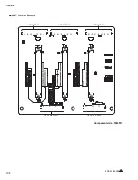
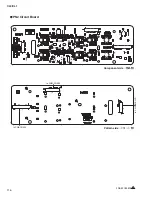
Page 95: ...95 CL3 CL1 CPU Circuit Board Pattern side to DSP CN101 2NA WY67750 1...
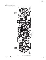
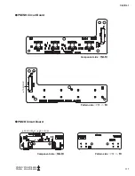
Page 101: ...101 CL3 CL1 DNTU Circuit Board Pattern side Scale 80 100 2NA WZ20390 5...
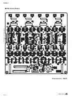
Page 102: ...CL3 CL1 102 2NA WY63530 FX Circuit Board WR 63 1 Component side Scale 95 100...
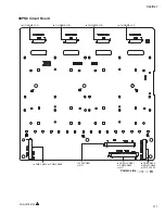
Page 103: ...103 CL3 CL1 2NA WY63530 FX Circuit Board Pattern side Scale 95 100...
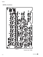
Page 105: ...105 CL3 CL1 HAAD Circuit Board Pattern side Scale 90 100 2NA WY64340 2...
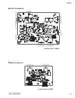
Page 107: ...107 CL3 CL1 2NA WY63490 Component side JK Circuit Board WR 63 1...
Page 109: ...109 CL3 CL1 Component side TBPHN Circuit Board WR 06 1 WR 63 1 2NA WY64360 1...
Page 110: ...CL3 CL1 110 Component side PN8 Circuit Board to FD8 CN902 or FD8CN CN902 2NA WY53120 2...
Page 118: ...CL3 CL1 118 Component side PNENL Circuit Board to PN8 CN001 2NA WY53130 1...
Page 160: ...CL3 CL1 160 1 18 LCD Test LCD LCD 1 3 2 9 5 OK NG 1 2 H 3 O X O 4 BOX 5x4...
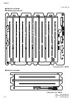
Page 382: ...7 MBCL CIRCUIT BOARDS A A A A 2NA WY53200 1 MB Circuit Board Component side...
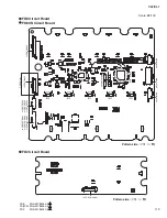
Page 383: ...MBCL 8 MB Circuit Board DSUB PH CONNECTOR ASSEMBLY B B B B 2NA WY53200 1 Pattern side...


