background image

MN5-0281-002

ii

Revision B

NOTICE

Copyright 2001, 2002, 2003, 2004

This document contains proprietary information that is protected by copyright. All rights 
are reserved. 

The information in this document is subject to change without notice. Please contact 
Xicom Technology for current technical specifications.

Xicom Technology reserves the right to revise this publication and to make changes 
from time to time in the content hereof without obligation of Xicom Technology to notify 
any person of such revision or changes.

Xicom Technology makes no warranty of any kind with regard to this material, including, 
but not limited to, the implied warranties of fitness for a particular purpose. Xicom 
Technology shall not be liable for errors contained herein or for incidental consequential 
damages in connection with the furnishing, performance, or use of this material.

Summary of Contents for XTS-200C

Page 1: ...cument The official version of this document is located in Xicom Technology Document Control Printed copies are for reference only 3550 Bassett Street Santa Clara CA 95054 USA 408 213 3000 Phone 408 2...

Page 2: ...Document Number MN5 0281 002 Date June 2004 Revision B XTS 200C Operation and Installation Manual...

Page 3: ...cument The official version of this document is located in Xicom Technology Document Control Printed copies are for reference only 3550 Bassett Street Santa Clara CA 95054 USA 408 213 3000 Phone 408 2...

Page 4: ...es the right to revise this publication and to make changes from time to time in the content hereof without obligation of Xicom Technology to notify any person of such revision or changes Xicom Techno...

Page 5: ...and Notes that are found throughout the manual Chapter Three Provides general installation information communication interface switch settings and cable pinouts Chapter Four Provides the operating ins...

Page 6: ...o should use this manual This manual is designed for use by trained operators and technicians who have a thorough knowledge of satellite transmitting and receiving equipment Persons using this manual...

Page 7: ...ifier Operation and Installation Manual Record of Changes Revision ECO Description Date Initiated By 1 Preliminary Release 07 15 2003 A L Crozier Jr A 12136 Original release 05 13 2004 A L Crozier Jr...

Page 8: ...dure SSPA MNC 0500 014 Preventive Maintenance MNC 0600 012 Chapter 7 Service and Repair MNC 0700 001 Appendix A Product Specifications 305 0281 002 Appendix B Mechanical Drawings Outline SSPA DC P S w...

Page 9: ...Release 04 17 2002 A L Crozier Jr A1 10179 Add numerous abbreviations 08 21 2002 A L Crozier Jr A2 10646 Add more abbreviations CE symbols 01 14 2003 A L Crozier Jr A3 11044 Add more abbreviations 05...

Page 10: ...MNC 0000 010 2 Revision A6...

Page 11: ...f Mechanical Engineers November 1999 ASME Y14 38 1999 Abbreviations and Acronyms Wachal Robert S 1999 Abbreviations Dictionary A practical compilation of today s acronyms and abbreviations Boston New...

Page 12: ...k CTRF center frequency CTS Clear to Send CW continuous wave DA digital to analog DAC digital to analog converter dB Decibel dBc Decibels referenced to carrier dBI Decibels referenced to Amperes or De...

Page 13: ...leakage HPA High Power Amplifier HV High Voltage Hz Hertz IC integrated circuit IESS Intelsat Earth Station Standards IF Intermediate Frequency I P Input inv inverter IPA Intermediate Power Amplifier...

Page 14: ...lector MSL mean sea level MTBF mean time between failures MTTR mean time to repair mV milli Volt MW Mega Watt mW milli Watt NAK negative acknowledgement oc overcurrent ODU Outdoor Unit OEM other equip...

Page 15: ...ique used to regulate the operating temperature environment of a device TPS Test Performance Sheet TWT Traveling Wave Tube TWTA Traveling Wave Tube Amplifier TXD Transmitted Data UMBC umbilical cord u...

Page 16: ...th Flat Display XTKH Xicom Technology Klystron High Efficiency Amplifier Flat Display with Multistage Depressed Collector XTRD Xicom Technology Rack Mount Digital Amplifier XTRD LDA Xicom Technology R...

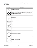
Page 17: ...s Acronyms and CE Symbols CE Symbols Symbol Definition Alternating Current AC CE Marking symbol for equipment and documentation meeting European Quality Standards Earth Ground Fuse Input Local OFF for...

Page 18: ...MNC 0000 010 10 Revision A6 List of Abbreviations Acronyms and CE Symbols Output Power OFF Power ON Protective Earth Ground Remote Reset Transmitted Power Monitor Symbol Definition...

Page 19: ...cription Date Initiated By 1 Preliminary Release 04 02 2002 A L Crozier Jr A 9869 Original Release 06 05 2002 A L Crozier Jr B 10033 Update to reflect amplifier improvement 08 05 2002 A L Crozier Jr C...

Page 20: ...tus Interface 3 Physical Characteristics 5 Environmental Specifications 5 Specifications 6 Contacting Xicom Technology 6 Assistance 6 Feedback 6 List of Figures Number Title Page Number Figure 1 Typic...

Page 21: ...g options are available a Block Upconverter a 1 1 redundant waveguide switch controller a 1 1 controller The COM1 interface is RS 232 only the COM2 interface is configured for RS 422 RS 485 operation...

Page 22: ...MNC 0100 007 4 Revision C Overview Figure 1 Typical Solid State Power Amplifier ODU Antenna Mount Block Diagram...

Page 23: ...appendix titled SSPA Power Supply Removal Procedure contains step by step instructions for removing the power supply module Environmental Specifications Table 1 Environmental Specifications lists the...

Page 24: ...ort email support xicomtech com Telephone 408 213 3109 24 Hours Facsimile 408 213 3107 Sales sales xicomtech com Feedback Xicom technology wants to receive customer feedback concerning the format cont...

Page 25: ...hanges Revision ECO Description Date Initiated By 1 Preliminary Release 04 02 2002 A L Crozier Jr A 9869 Original Release 06 05 2002 A L Crozier Jr B 12217 Add Fuse and Power Receptacle Warnings 05 18...

Page 26: ...ngs Cautions and Notes 3 General Warnings and Cautions 5 High Voltage Hazards 5 Ladder Hazards 6 RF Radiation Hazards 7 Sicherheit 8 Allgemeine Information 8 Zusammenfassungen 8 Beschreibung 8 Warnung...

Page 27: ...ied in this chapter are applicable to anyone doing the procedures included in this manual Warnings Cautions and Notes Warnings cautions and notes are used in these procedures to alert the user to spec...

Page 28: ...ersonnel could result from radio frequency burns WARNING This symbol denotes a LADDER FALL HAZARD WARNING in a procedure step and is used whenever death or injury to personnel could result from improp...

Page 29: ...ar with safety precautions related to DOUBLE POLE NEUTRAL FUSING Failure to comply could result in serious injury or death WARNING The Solid State ODU power amplifier is not equipped with internal saf...

Page 30: ...quipment OFF use shorting probe to ensure capacitors are discharged ensure meter probes are properly insulated and capable of handling voltages of 1 kv or more attach probes using one hand ensure prob...

Page 31: ...igned to perform the maintenance does not wear a pacemaker all the microwave connections are securely fastened that there is no microwave leakage Failure to comply could result in serious injury or de...

Page 32: ...fahren durchf hrt Warnungen Ermahnungen zur Vorsicht und Beachtungshinweise In diesen Verfahren werden Warnungen Ermahnungen zur Vorsicht und Beachtungshinweise verwendet um den Benutzer auf besondere...

Page 33: ...EFAHR DURCH HOCHFREQUENZ bei einem Verfahrensschritt und wird immer dann verwendet wenn der Tod oder die Verletzung von Menschen durch von Hochfrequenz hervorgerufene Verbrennungen verursacht werden k...

Page 34: ...der Beachtung bei der Durchf hrung eines oder mehrerer Verfahrensschritte erfordert Hinweis Dieses Symbol bedeutet einen HINWEIS bei einem Verfahrensschritt Ein HINWEIS wird immer dann verwendet wenn...

Page 35: ...tfernt wird werden mehrere unter Hochspannung stehende Punkte freigelegt Seien Sie extrem vorsichtig wenn Sie den Verst rker ohne Abdeckung betreiben Nichtbeachtung k nnte zu ernsthaften Verletzungen...

Page 36: ...ern Sie sich dass die Sonden keine anderen Kontakte ber hren Nichtbeachtung k nnte zu ernsthaften Verletzungen oder Tod f hren Leitergefahren WARNUNG Wenn Sie eine Leiter ben tzen m ssen vergewissern...

Page 37: ...g eingeteilte Techniker keinen Herzschrittmacher tr gt alle Mikrowellenverbindungen sicher befestigt sind keine Mikrowellen austreten k nnen Nichtbeachtung k nnte zu ernsthaften Verletzungen oder Tod...

Page 38: ...MNC 0200 004 14 of 14 Revision C Safety Sicherheit...

Page 39: ...date Fault Indicators 08 05 2002 A L Crozier Jr C 10197 Update RF Inhibit Information 08 26 2002 A L Crozier Jr D 10490 Update to reflect waveguide flange protection 12 10 2002 A L Crozier Jr E 12103...

Page 40: ...AMP Select J1 d 14 Re program Computer J1 e 14 Summary Fault Dry Contact J1 S to J1 X 14 Output Voltages 15 J1 b C 15 J1 g 15 RF Inhibit control 15 RF Inhibit with Internal Source 15 RF Inhibit with...

Page 41: ...igure 6 A B Amplifier select 14 Figure 7 RF Inhibit with Internal Source 15 Figure 8 RF Inhibit with External Source 16 Figure 9 RF Inhibit with switch A opened 17 Figure 10 Waveguide Connector Pin La...

Page 42: ...Unpacking and Installation List of Tables Number Title Page Number Table 1 Digital Monitor and Control Connector J1 Pinouts 12 Table 2 Analog Monitor and Control Connector Pinouts 13 Table 3 J6 Wavegu...

Page 43: ...pping container and packing material and use it if you need to reship the unit Inspection Inspect all items for any damage received during shipment If shipping damage is detected submit a damage repor...

Page 44: ...rear panel of the amplifier Ensure that the proper matching waveguide flange is used to connect the amplifier input and output to the RF load Refer to Figure 1 Typical 4 Screw Mounting Flange Tighteni...

Page 45: ...utilized to eliminate potential strain on the waveguide connection 3 Insert any necessary gaskets and windows between the two flanges Note If the connecting waveguide is to be pressurized at greater t...

Page 46: ...ifier is cooled with a built in fan Heated exhaust air should not be recirculated into the power amplifier A clearance of 6 8 inches is recommended to allow the heated exhaust air to clear the power a...

Page 47: ...rate when the AC line voltage is anywhere in the specified range Figure 3 shows the pinouts for a low power ODU Figure 3 Connector J2 Pinout for Low Power Unit Refer to the Outline Drawing in the appe...

Page 48: ...rt Two sets of Form C Relay contacts for Summary Fault indication RF Inhibit Control 24 VDC 100 mA maximum 15 VDC for monitoring purposes only Hardware Address Select digital SSAs only Monitor and Con...

Page 49: ...MNC 0300 011 11 of 26 Revision H Unpacking and Installation Figure 5 Analog M C Connector Pin Layout...

Page 50: ...ummary Fault B Normally Open Contact V Closed to X when Fault W Summary Fault B Normally Closed Contact W Opened to X when Fault X Summary Fault B X Summary Fault B Common Y RF Inhibit Opto isolator L...

Page 51: ...to Low Transmit ON J Transmit Select OFF Opto Low Transmit OFF K Fault Reset Opto Low Reset L External Interlock 1 Normally Opto Low Open Hi Fault M External Interlock 2 Normally Opto Low Open Hi Faul...

Page 52: ...cted Otherwise amplifier address A is selected Figure 6 A B Amplifier select Re program Computer J1 e Connect this input low to pin Z or a to update firmware To update firmware please refer to Firmwar...

Page 53: ...ailable on Pin f The return for this voltage is either Pin a or Pin Z RF Inhibit control The HPA has the capability to Inhibit RF If the unit has a SSA preamplifier inhibit is accomplished by turning...

Page 54: ...und usseren Referencen nucht mischen Die Nichtbeachtung kann zu Sch den am Ger t F hren Refer to Figure 8 J1 g can be driven from an external voltage source of 5 to 15 VDC In this case J1 Y should be...

Page 55: ...voltage correspondence to the RF output power The conversion formula is Vo 10 PdBm 47 27 19 05 or PdBm 47 27 19 05 log10 Vo With PdBm RF Output power in dBm Waveguide Switch connection Digital SSPAs O...

Page 56: ...Table 3 J6 Waveguide Switch Connector Pinouts PIN Description A WG SW1 SEL A B WG SW1 SEL B C WG SW2 SEL A D WG SW2 SEL B E WG SW1 POS A IND F WG SW1 POS B IND G WG SW1 RF Inhibit H WG SW2 POS A IND J...

Page 57: ...on is selected a 24 V pulse will be sent to the WG Switch to initiate the switch rotation Figure 11 WG SW1 Position A Select Command WG Switches Position Indicator Refer to Figure 12 The WG Switch pos...

Page 58: ...ides a pull up resistor of 100K to 15V for an open collector input at J6 M A logic HI is present when the other amplifier faults or is turned off Figure 13 Sum Fault Input Sum Fault Output Refer to Fi...

Page 59: ...he Waveguide Switch RF Inhibit input provides a pull up resistor of 100K to 15V An input HI is required when a RF Inhibit command is received from Waveguide Switch 1 at J6 G or Waveguide Switch 2 at J...

Page 60: ...will take its place This automatic switching requires that the backup amplifier must be operational not faulted and in automatic mode Please refer to the system manual for more details on redundant s...

Page 61: ...mmand received has precedence COM1 is an RS 232 only serial interface No switch settings are required for COM1 Table 1 Digital Monitor and Control Connector J1 Pinouts on page 12 lists the pinouts for...

Page 62: ...ications Refer to the specification in Appendix A for detailed specifications of your apmplifier Grounding WARNING To prevent Electric Shock the amplifier should be securely connected to the grounding...

Page 63: ...turn AC input power ON or OFF There is also a LED indicator on the amplifier front panel Depending on the state of the amplifier this indicator shows AMBER when the unit is in standby GREEN when tran...

Page 64: ...MNC 0300 011 26 of 26 Revision H Unpacking and Installation...

Page 65: ...evision ECO Description Date Initiated By 1 Preliminary Release 04 02 2002 A L Crozier Jr A 9869 Original Release 06 05 2002 A L Crozier Jr B 10033 Update to reflect amplifier improvement 08 05 2002 A...

Page 66: ...lt Mode 3 Summary Fault 3 Power Supply Voltage Fault 4 SSPA Overtemperature Fault 4 Reverse Power Fault 4 Clearing Faults 4 Control and Status Signals 5 Control Signals 5 AC Power ON 5 Normal M C Inte...

Page 67: ...ng Modes There are three amplifier operating modes Standby Transmit ON Fault Standby Mode In this mode the SSPA is ready for main voltage to be applied Transmit ON Mode When transmit is enabled applie...

Page 68: ...erature of the base plate is reduced to a safe operating level Power supply voltage will automatically be enabled when the over temperature fault clears Note An over temperature fault should be cause...

Page 69: ...d through the system interface All commands are identified in the chapter titled SSPA Communications and Protocol Manual In manual operation the SSPA is turned ON by connecting the AC Cord to the prim...

Page 70: ...r input connector pins must be used dependent on voltage level and the prime power source Refer to the appendix titled Mechanical Drawings for connector pin outs 2 The amplifier is installed within an...

Page 71: ...stem is held in the reset mode until the J1 Pin h is connected to either J1 Pin Z or J1 Pin a This allows the control system to operate normally Note In manual operation the system is configured to tr...

Page 72: ...Operation MNC 0400 012 8 of 8 Revision C...

Page 73: ...s Revision ECO Description Date Initiated By 1 Preliminary Release 04 02 2002 A L Crozier Jr A 9869 Original Release 06 05 2002 A L Crozier Jr B 10523 Update to reflect change in specifications 12 06...

Page 74: ...and Protocol 5 Overview 5 Communication 5 Digital SSPA Solid State Power Amplifier 5 Compatibility 6 Protocol 7 Overview 7 Message Format 7 RS 485 7 Printable vs Non Printable Protocols 8 Communicati...

Page 75: ...MNC 0500 010 3 Revision D Solid State Power Amplifier Communication and Protocol List of Figures Number Title Page Number Figure 1 Basic Configuration 6...

Page 76: ...List of Tables Number Title Page Number Table 1 Standard Packet Format 9 Table 2 Packet Format Redundant Controller XTSC 100 Family 9 Table 3 Start Byte End Byte Check Byte 9 Table 4 Check Byte Calcu...

Page 77: ...a serial interface The term digital refers to devices with a serial interface RS 232 RS 485 Xicom amplifiers typically respond to a message in less than 20 milliseconds Communication Digital SSPA Sol...

Page 78: ...ility Two serial hardware interfaces RS 232 RS 422 485 are available for the control link Amplifiers without the power monitor option will respond to queries for power readings but the value returned...

Page 79: ...ly communicate with individual devices that are sharing a RS 485 bus Each message has a mandatory message byte followed by a variable number of parameters Some messages have no parameters while others...

Page 80: ...ed to indicate whether a message was accepted or rejected For nearly all implementations the non printable protocol should be used If you send a message using the printable protocol devices will respo...

Page 81: ...essage Byte Parameters as Required End Byte Check Byte Table 2 Packet Format Redundant Controller XTSC 100 Family Start Byte Address Byte Device Selection Byte Message Byte Parameters as Required End...

Page 82: ...4 32 76 ASCII L Example of Exclusive OR Algorithm Message ID Version Query STX A 0 ETX ASCII Progressively XORs the bytes to establish the check byte Check byte STX A 0 ETX ASCII character may be non...

Page 83: ...generating the commands and queries of the protocol Table 5 Command Reject Codes ASCII Character Reject Reason a Command byte not recognized b Illegal parameter or parameter out of range c System in...

Page 84: ...095 5F LF 010 0A 5 053 35 096 60 VT 011 0B 6 054 36 a 097 61 FF 012 0C 7 055 37 b 098 62 CR 013 0D 8 056 38 c 099 63 SO 014 0E 9 057 39 d 100 64 SI 015 0F 058 3A e 101 65 DLE 016 10 059 3B f 102 66 DC...

Page 85: ...6 033 21 L 076 4C w 119 77 034 22 M 077 4D x 120 78 035 23 N 078 4E y 121 79 036 24 O 079 4F z 122 7A 037 25 P 080 50 123 7B 038 26 Q 081 51 124 7C 039 27 R 082 52 125 7D 040 28 S 083 53 126 7E 041 29...

Page 86: ...number V is the firmware version number RR is the firmware revision level Optional Parameter 0 Returns the following Response MMMM MMM SSSSS V RR YYYY MM DD MMMM MMM is the amplifier model number SSSS...

Page 87: ...ways zero 6 Complement of Bit 5 5 Summary Fault 4 Reserved 3 Reserved 2 Alarm Exists 1 Reserved 0 Reserved Notes Power Supply Enabled is only defined for amplifiers connected to a controller If you qu...

Page 88: ...onverter Fault 3 Over Temp Fault 2 Reserved 1 Fan Locked 0 Low Line Byte B Bit 7 Reserved always zero 6 Complement of bit 5 5 Power Supply Fault 4 High Reflected Power 3 External Interlock open 2 Low...

Page 89: ...t string in the sequence is followed by an additional Compatibility Not available when querying amplifiers through controllers Current Screen Command Byte 5 Response Returns the amplifier s current sc...

Page 90: ...ols the attenuator Alarm Condition Command Byte 9 Response One byte of alarm status formatted as follows Bit 7 Reserved always zero 6 Complement of bit 5 5 High Output Power 4 Low Output Power 3 High...

Page 91: ...Interface Up Down status I IP Address N Netmask M MAC Address U Interface Up Down status Examples Query PED Returns PEDX where X 1 if interface is Down disabled or 0 if interface is Up enabled Query...

Page 92: ...er to construct custom query sequences It is a complete polling solution returning virtually any measurement you might want Measurements are requested via a variable length parameter list The length o...

Page 93: ...2 Pos B Bit 3 Switch 2 Pos A Bit 2 automatic mode Bit 1 Waveguide Switch Position 0 other amplifier Bit 0 Waveguide Switch Position 1 this amplifier Byte D Bit 7 Reserved Always 0 Bit 6 Compliment of...

Page 94: ...Bit 3 Reserved Bit 2 Reserved Bit 1 Reserved Bit 0 Reserved Byte D Bit7 Reserved Bit6 Compliment of Bit5 Bit5 Reserved Bit4 Reserved Bit3 Reserved Bit2 Reserved Bit1 Reserved Bit0 Reserved 1 Summary S...

Page 95: ...A XXXX in Watts generate alarm F XXXX in Watts generate fault D XXXX in Watts disabled M Supply Hours XXXXXX hours N Transmit Hours XXXXXX hours P Fwd Power XX X in dBm Q Reverse Power XX X in dBm R...

Page 96: ...n COM2 R returns RS 485 Configuration Response for 1 and 2 CBBBBBBPDS C Communications port 1 COM1 2 COM2 COM1 RS 232 port COM2 RS 485 port BBBBBB Current baud rate Example 019200 P Parity N O or E D...

Page 97: ...rated Parameter YYYY MM DD HH MM Note The Hour is in 24 hour format Unit does not reply to this command Reset Command Byte Function Resets the unit Note Unit does not reply to this command VDD Voltage...

Page 98: ...to use a Go To Power command D or E Parameter XXXX steps This is an integer preceded by or This offset is applied to the current attenuator count which ranges from 0 to 4095 Note If direct attenuation...

Page 99: ...lity Attenuator required Constant Power Watts Command Byte G Function The SSPA seeks the specified power level until Constant Power is terminated by Goto Power Command Byte D or E or Terminate Constan...

Page 100: ...SSPA Response Resulting attenuation in XX X dB If the user specified an attenuation value outside the attenuator s range the closest valid value will be used Note Use this to find max attenuation For...

Page 101: ...t D to disable XXXX is the desired trip point in Watts Reflected RF Trip Command Byte O Function Sets a Reflected RF trip point If reflected power exceeds the set point an alarm or fault is generated...

Page 102: ...sable X 1 to enable Parameter JXX to set ambient room temperature in degrees C XX 20 to 60 C Parameter EX X is the Ethernet mode or parameter you wish to set D Bring interface Down disable U Bring iin...

Page 103: ...5 port BBBBBB Desired baud rate 038400 019200 009600 004800 002400 001200 P Parity N O or E D Data bits 8 or 7 S Stop bits 1 Parameter Format 2 RABC Response ABC A 4 or 2 Wire B T Terminated or U Unte...

Page 104: ...MNC 0500 010 32 Revision D Solid State Power Amplifier Communication and Protocol...

Page 105: ...Firmware Update Procedure HPA Record of Changes Revision ECO Description Date Initiated By 1 Preliminary Release 11 21 2002 A L Crozier Jr A 12182 Original Release 05 04 2004 A L Crozier Jr B 12760 Up...

Page 106: ...A Table of Contents Paragraph Title Page Number Firmware Update Procedure HPA 3 Overview 3 Required Items 3 Updating HPA Firmware 4 Reject Codes 6 List of Figures Paragraph Title Page Number Figure 1...

Page 107: ...the appendix titled Firmware The middle four digits XXXX of the 803 correspond to the middle four digits XXXX of the 808 part number 800 XXXX XXX Bill of material for the files required to operate yo...

Page 108: ...the RS 232 connector of the HPA control cable 2 Set the programming switch on the control cable to the program position 3 Place the firmware executable file and the coldloader bin pilot bin and flash...

Page 109: ...r the complete path where the three loader files are stored or click on the buttons with the three dots and browse to the directory where the files are located and select that file Press OK Figure 2 L...

Page 110: ...ck on the three dots button and browse to the directory where the firmware executable file is located and select that file Press OK Figure 4 Locate the Flash Image File 9 The Rfu application will begi...

Page 111: ...e ODU SSPA Record of Changes Revision ECO Description Date Initiated By 1 Preliminary Release 03 11 2003 A L Crozier Jr A 12302 Original Release 06 16 2004 A L Crozier Jr B 10910 Update Chapter Title...

Page 112: ...ge Number Preventive Maintenance ODU SSPA 3 Requirements 3 Monthly 3 Quarterly 3 Maintenance Procedures 3 Fin Assembly 3 Battery Disposal Instructions 4 General Information 4 Europe 4 United States 4...

Page 113: ...supply fins Maintenance Procedures Fin Assembly Perform the following procedure to remove inspect and clean the cooling Fin Assembly 1 Turn the Power Amplifier OFF 2 Disconnect the Prime Power 3 Remov...

Page 114: ...by each member country Therefore in each country the manufacturers importers and users are responsible for the proper disposal or recycling In accordance with these directives the TL 5242 W battery c...

Page 115: ...ch einen autorisierten Entsorgungsbetrieb erfolgen welcher mit den Bundes Landes und rtlichen Vorschriften zum Transport und der Entsorgung von Gefahrstoffen vertraut ist Wir empfehlen Ihnen sich mit...

Page 116: ...cht kommende Metall der Zelle ist das Lithium das nicht auf der Liste gef hrt oder als giftiger Sonderm ll eingestuft ist Gr ere Mengen unbehandelter und nicht v llig entladener verbrauchter Zellen we...

Page 117: ...Figures List of Tables 09 2001 A L Crozier Jr A 9183 Original Release 10 12 2001 A L Crozier Jr B 9359 Delete figure 1 and attach RMA Form PDF at end of chapter 11 27 2001 A L Crozier Jr C 9395 Remov...

Page 118: ...r Table of Contents Paragraph Title Page Number Service and Repair 3 Introduction 3 Return Authorization 3 Returned Material Authorization 3 Shipping Information 4 Figure 1 RMA Request Form Example 5...

Page 119: ...maintenance manuals are provided to all personnel who complete the equipment operation and repair training program The maintenance manuals include all the necessary documents to service and repair Xic...

Page 120: ...ugated boxes Ensure there is adequate packing material between the equipment and the outside box Seal the container with heavy packing tape or metal bands Mark the container with the words FRAGILE DEL...

Page 121: ...we have a purchase order in place Price for this repair Includes all repair parts labor upgrades and full testing Purchase order number TWT and Linearizer Excluded they will be quoted on a parts and...

Page 122: ...MNC 0700 001 6 Revision F Service and Repair...

Page 123: ...ge Aoppendix A 05 09 2005 JT 12889 A Rev change only 03 29 2005 Judy N A 1 Create document 12 16 2004 LS ECN REV DESCRIPTION DATE APPROVED XTS 200C 5 85 6 425GHz Document No 305 0281 002 REV B Page 1...

Page 124: ...SPECIFICATIONS 3 1 ELECTRICAL INTERFACE 3 1 1 RF Output CPRG 137 3 1 2 RF Input Type N female 3 1 3 Sample Port Type N female 3 1 4 Monitor Control 32 pin MS3114E 18 32SW 3 1 5 Waveguide Switch Contro...

Page 125: ...5 6 Gain Variation with 2 dB over 40 to 50 deg C Temperature 3 2 6 Noise Figure 8 dB maximum 3 2 7 Noise Power In Band 80 dBW 4 kHz maximum 3 2 8 Noise Power Receive Band 150 dBW 4 kHz maximum 3 7GHz...

Page 126: ...Spurious Signals 65 dBc out of band 3 2 16 Sample Port Coupling 40 dB nominal 3 2 17 Power Requirements Prime Power 90 264 VAC 47 63Hz single phase 1250 VA typical 1600 VA maximum 0 95 Power Factor 3...

Page 127: ...to 70 Deg C 3 4 1 2 Vibration When packed in original shipping containers or mounted to a rigid support structure MIL STD 810F Method 514 5 Procedure I two hours per axis using the following PDS curve...

Page 128: ...ximum 3 6 GENERAL REQUIREMENTS 3 6 1 Quality Assurance Quality standards will meet ISO 9000 4 0 OPTION FEATURES 4 1 Waveguide Switch Control 5 0 TESTING REQUIREMENTS 5 1 Acceptance Test Procedure ATP...

Page 129: ...s Spec Paragraph No Test Description Test Condition Min Max Units Measured Performance Pass or Fail 3 2 1 Frequency Translation Frequency Fout Fout 4 9GHz IF Fout 5 85GHz 6 00GHz 6 1275GHz 6 425GHz No...

Page 130: ...STD Output freq swept from 5 85 to 6 425 GHz NA 0 04 dB MHz See attached plot Pass Fail 3 2 5 5 Gain Control Note 2 and Set Attn to 20 dB STD Output freq swept from 5 85 to 6 425 GHz 20 N A dB Pass F...

Page 131: ......

Page 132: ......

Page 133: ......

Page 134: ......

Page 135: ......

Page 136: ......

Page 137: ......

Page 138: ......

Page 139: ......

Page 140: ......

Page 141: ...ODU SSPA Power Supply Removal ODU SSPA Power Supply Removal Record of Changes Revision ECO Description Date Initiated By 1 Preliminary Release 04 12 2004 A L Crozier Jr 2 Update to reflect new power s...

Page 142: ...Title Page Number ODU SSPA Power Supply Removal 5 Overview 5 Required Tools and Materials 5 Removing Power Supply Part Number 310 0476 001 6 Replacing Power Supply Part Number 310 0476 001 8 Removing...

Page 143: ...ge Number Figure 1 Location of Power Supply Screws 6 Figure 2 Power Supply Interface Connectors 7 Figure 3 Power Supply Interface Connector Key and Slot Location 8 Figure 4 Location of Power Supply Sc...

Page 144: ...MNC 0000 039 4 of 12 Revision 2 ODU SSPA Power Supply Removal...

Page 145: ...y may be removed and replaced while the amplifier is in place or it may be done at a repair facility Required Tools and Materials A 2 Phillips Head Screwdriver is the only tool required to remove and...

Page 146: ...procedure to remove the power supply Part Number 310 0476 001 1 Turn the amplifer power OFF Remove the input power cable 2 Refer to Figure 1 Turn the amplifier upside down 3 Using a 2 Phillips Head Sc...

Page 147: ...nterface Connectors Note Each of the interface connectors on the amplifier are attached to cables that retract into the amplifier case This makes connecting and disconnecting the power supply simple 5...

Page 148: ...lifier and power supply Line up the connector key slots with the key on the power supply connectors Connect the power supply to the interface connectors Line up the red locking guide dots on the inter...

Page 149: ...Number 310 0415 003 Use this procedure to remove the SSPA power supply Part Number 310 0415 003 1 Turn the amplifer power OFF Remove the input power cable 2 Refer to Figure 4 Turn the amplifier upside...

Page 150: ...y clear of the amplifier case and place it on a flat surface Replacing Power Supply Part Number 310 0415 003 Use this procedure to replace the SSPA power supply Part Number 310 0415 003 1 Refer to Fig...

Page 151: ...ace connector with the locking guide tracks on the power supply connector Screw the interface connector on to the power supply connector 3 Carefully slide the power supply in until the heatsink fits i...

Page 152: ...MNC 0000 039 12 of 12 Revision 2 ODU SSPA Power Supply Removal...

Page 153: ...ation Addendum SSPA M C Termination Cable Record of Changes Revision ECO Description Date Initiated By 1 Preliminary Release 12 04 2002 A L Crozier Jr A 12182 Original Release 05 04 2004 A L Crozier J...

Page 154: ...have all the functions setup properly disconnect the Controller M C cable from the SSPA J1 and replace it with the termination cable The SSPA will now operate unattended Termination Cable Wiring Pin...

Page 155: ...MNC 0000 003 3 of 4 Revision B Operation Addendum SSPA M C Termination Cable...

Page 156: ...MNC 0000 003 4 of 4 Revision B Operation Addendum SSPA M C Termination Cable...

Page 157: ...otocol Addendum Block Upconverter Protocol Addendum Block Upconverter Record of Changes Revision ECO Description Date Initiated By 1 Preliminary Release 12 14 2001 A L Crozier Jr A 9474 Original Relea...

Page 158: ...MNC 0000 002 2 Revision A Protocol Addendum Block Upconverter Table of Contents Paragraph Title Page Number Protocol Adendum Block Upconverter 3 Block Upconverter Protocol 3...

Page 159: ...ence frequency or indicate malfunction in the system PLL Phase Lock Loop If the reference frequency is not present the HPA High Power Amplifier in the system shuts down by disabling the high voltage s...

Page 160: ...MNC 0000 002 4 Revision A Protocol Adendum Block Upconverter...

Page 161: ...Upconverter Record of Changes Revision ECO Description Date Initiated By A 10125 Original Release 08 05 2002 A L Crozier Jr B 10516 Add X and DBS Band Information 12 06 2002 A L Crozier Jr C 12612 Ad...

Page 162: ...p and Turn On 6 Reference Oscillator Drift Compensation 7 Figure 1 Typical Block Diagram of a High Power Amplifier with Block Upconverter 3 Figure 2 Reference Frequency Phase Noise Chart 4 Figure 3 De...

Page 163: ...overall system stability and phase noise A typical phase noise requirement for a reference source is shown in Figure 1 The phase noise of the modem input signal at the IF frequency also affects the s...

Page 164: ...esizer and IF frequency to the mixer The synthesizer generates the LO frequency from the reference frequency and filters it to eliminate unwanted harmonics The LO is amplified and passed to the LO por...

Page 165: ...MNC 0000 015 5 of 8 Revision C Operation Addendum Block Upconverter Figure 3 Detailed BUC Block Diagram...

Page 166: ...us signals such as IF and reference frequency products must be below 60 dBc The output frequency accuracy depends on the accuracy of the refer ence and IF frequencies The determining ratios for the fr...

Page 167: ...gh voltage circuit Note The power levels and frequencies discussed in the paragraphs above are representative of typical BUC performance The specific power levels and frequencies that the BUC in the H...

Page 168: ...MNC 0000 015 8 of 8 Revision C Operation Addendum Block Upconverter Figure 4 Drift Compensation Block Diagram...

Reviews: