October 2012
8-15
ColorQube 8570/8870 Service Manual
Printer Electronics
Theory of Operation
Xerox Internal Use Only - Revised, 3rd Revision
Wave Amplifier
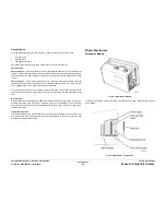
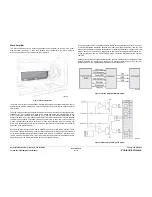
The Wave Amplifier serves as a high-voltage linear power amplifier for the VPP/ VSS gener-
ated waveform transducer to drive the Printhead load requirements. The Wave Amp also
drives all active piezo-electric transduces (PZT) elements.
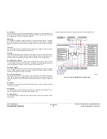
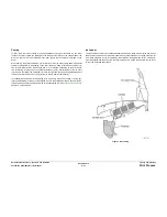
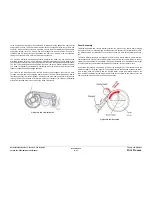
Figure 12 Wave Amplifier
The Wave Amp includes two independent discrete high-voltage linear power amplifiers, one for
generating the positive polarity VPP pulses and another for generating the negative polarity
VSS pulses.
The high-voltage linear power amplifier design features an AC-coupled driver topology with DC
feedback. The AC coupled drive is good for the pulsed application and provides high current
drive for fast slew rates while maintaining good recovery and transient performance. The
design also has a "near zero" control switch that provides DC restoration for the drive coupling
capacitors and activates a secondary feedback control loop to drive and hold the output at
ground potential that otherwise would result in "open loop" operation when not pulsing. The
Wave Amp also has an enable control as well as over-current fault detection. Each polarity
driver has a Temperature Sensor.
Both polarity driver designs utilize power MOSFETs as the principle driving devices. These
devices are capable of supplying the large currents required for driving several PZT elements
at the required bandwidths with relatively simple drive circuitry. The MOSFET devices are uti-
lized in a feedback amplifier circuit to provide controlled, linear waveform amplification and to
buffer the drive for the control waveforms derived from system memory.
The pulse sequences for the different polarity drivers are asymmetrical and result in non-uni-
form power dissipation distribution between the similar linear power amplifiers. Thus, the VSS
driver power dissipation is primary limiting factor for thermal performance. The four VPP/VSS
MOSET devices are mounted on a large common heat sink with the VSS MOSFET drains con-
tacting the heat sink and the VPP MOSFETs drains electrically insulated from the common
heat sink.
Although this approach would allow simultaneous opposite polarity pulses, the differential input
voltage limitations for the ASIC and the desire for maximum drive result in using only one
polarity pulse at a time, appropriately selected by the print head ASIC.
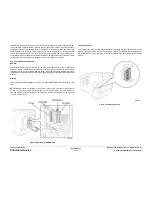
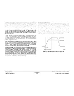
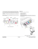
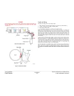
Figure 13 Wave Amplifier Block Diagram
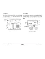
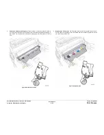
Figure 14 Wave Amplifier Signal Diagram
Summary of Contents for COLORQUBE 8570
Page 1: ...ColorQube 8570 8870 Printer ColorQube 8570 8870 Service Manual Xerox Internal Use Only...
Page 2: ......
Page 423: ......

