


CH32V003
Reference Manual
V1.3
90
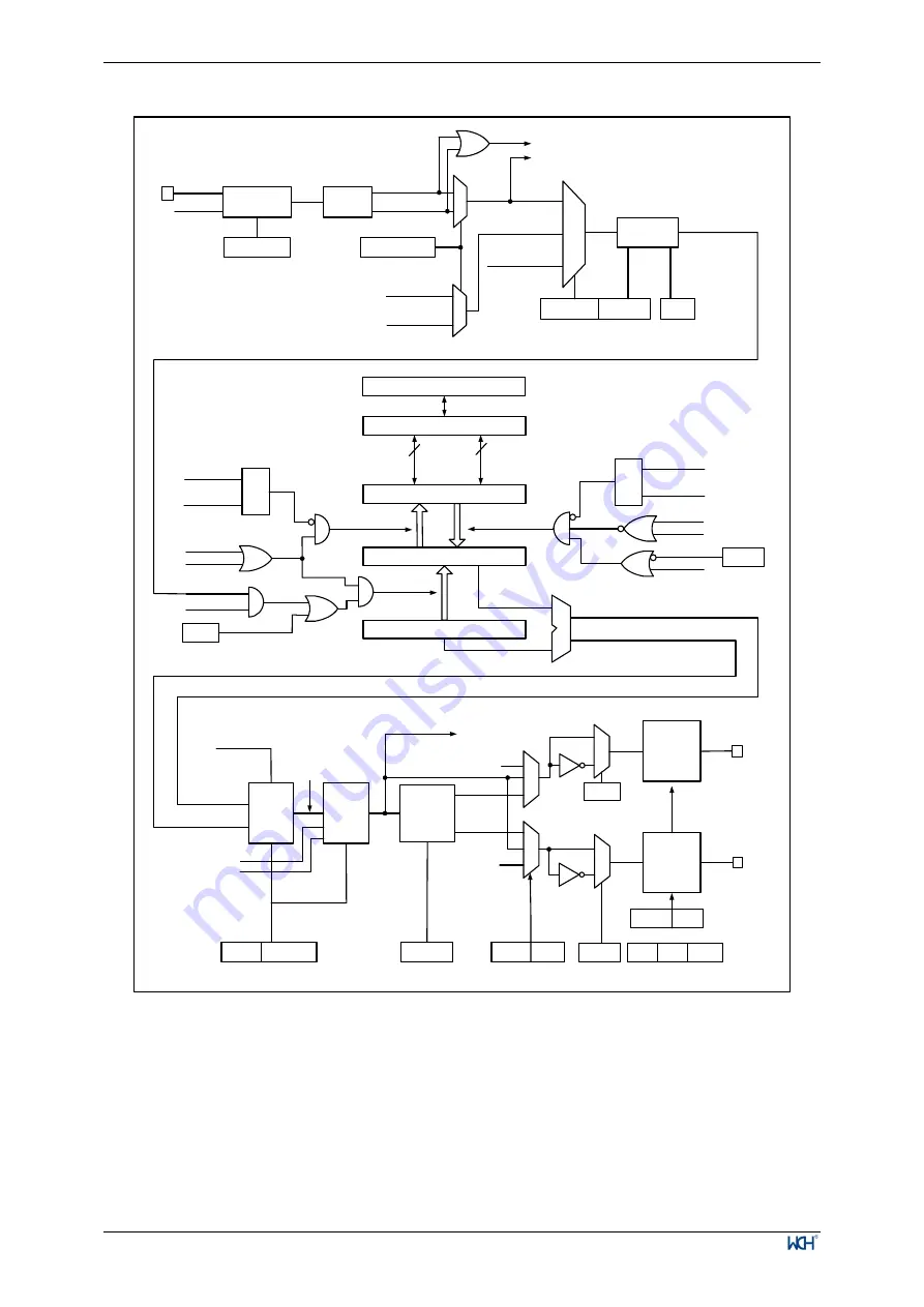
Figure 10-3 Block diagram of the structure of the comparison capture channel
The structure block diagram of the comparison capture channel is shown in Figure 10-3. The signal is input
from the channel x pin and optionally made as TIx (the source of TI1 can be more than just CH1, see the
structure block diagram of timer 10-1), TI1 is passed through the filter (ICF[3:0]) to generate TI1F, and then
divided into TI1F_Rising and TI1F_Falling through the edge detector, these two signals are selected (CC1P)
to generate TI1FP1, TI1FP1 and TI2FP1 from channel 2 are sent together to CC1S to select to become IC1,
which is sent to the comparison capture register after ICPS dividing.
The compare capture register consists of a preload register and a shadow register,
and the read/write process
operates only on the preload register. In capture mode, the capture occurs on the shadow register and is then
copied to the preload register; in compare mode, the contents of the preload register are copied to the shadow
register, and then the contents of the shadow register are compared to the core counter (CNT).
0
1
01
10
11
TI1F
Edge
detector
ICF[3:0]
TIMx_CHCTLR1
TI1F_Rising
TI1F_Falling
To the slave mode controller
TI1F_ED
TI1FP1
CC1P/CC1NP
TIMx_CCER
TI2F_Rising
TI2F_Falling
0
1
(from channel 2)
(from channel 2)
TI2FP1
TRC
(from slave mode
controller)
Divider
/1,/2,/4,/8
IC1
CC1S[1:0] ICPS[1:0]
CC1E
TIMx_CHCTLR1 TIMx_CCER
Filter
downcounter
TI1
f
DTS
APB Bus
MCU-peripheral interface
Capture/compare preload register
Capture/compare shadow register
hi
gh
8
(if
16
-b
it)
low
8
Capture
Counter
CC1G
TIM1_SWEVGR
CC1E
IC1PS
CC1S[0]
CC1S[1]
S
R
Read CCR1H
Read CCR1L
read_in_progress
capture_transfer
Input
mode
compare_transfer
Output
mode
S
R
write_in_progress
Write CCR1H
Write CCR1L
CC1S[0]
CC1S[1]
OC1PE
OC1PE
UEV
TIM1_CHCTLR1
(from time
base unit)
Comparator
CNT
>
CCR1
CNT = CCR1
Output
mode
controller
ETRF
OC1REF
OCxREF
OCxREF
OC1CE OC1M[3:0]
Output
selector
Dead-time
generator
x0
01
11
11
10
0x
To the master mode
controller
OC1REFC
‘
0
’
OC1N_DT
OC1_DT
‘
0
’
0
1
Output
enable
circuit
OC1
CC1P
TIM1_CCER
0
1
Output
enable
circuit
OC1N
TIM1_CCER
DTG[7:0]
TIM1_BDTR
TIM1_CCER
CC1NE CC1E
CC1NP
TIM1_CCER
CC1NE CC1E
TIM1_BDTR
MOE OSSI OSSR
TIM1_CHCTLR1


