


CH32V003
Reference Manual
V1.3
113
can also be output as TRGO to other peripherals such as timers and ADCs.
The core of the general-purpose timer is a 16-bit counter (CNT). cK_PSC is divided by a prescaler (PSC) to
become cK_CNT and then finally fed to the CNT, which supports incremental counting mode, decremental
counting mode, and incremental and decremental counting mode, and has an auto-reload register (ATRLR) to
reload the initialization value for the CNT at the end of each counting cycle.
The universal timer has four sets of compare capture channels, each of which can input pulses from exclusive
pins or output waveforms to pins, i.e., the compare capture channels support both input and output modes. The
input of each channel of the compare capture register supports filtering, dividing, edge detection, and other
operations, and supports mutual triggering between channels, and can also provide clock for the core counter
CNT. Each comparison capture channel has a set of comparison capture registers (CHxCVR) that support
comparison with the main counter (CNT) to output pulses.
11.2.2 Difference between general-purpose timer and advanced-control timer
Compared to advanced-control timers, general purpose timers lack the following features.
1)
The general-purpose timer lacks a repeat count register for counting the count cycles of the core counter.
2)
The comparison capture channel of the general-purpose timer lacks deadband generation and has no
complementary output.
3)
The generic timer does not have a brake signal mechanism.
4)
The default clocks CK_INT for general-purpose timers are all from APB1, while the CK_INT for
advanced-control timers are all from APB2.
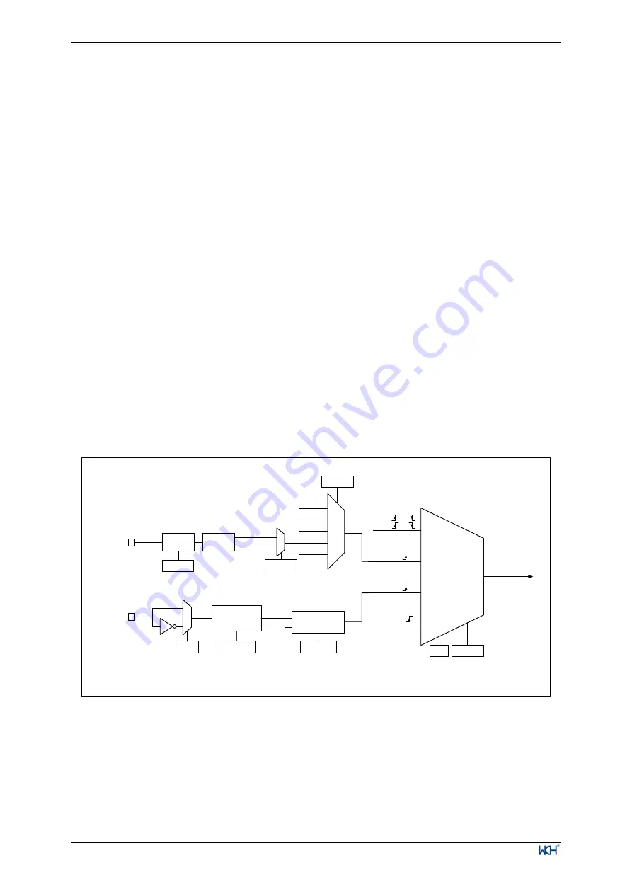
11.2.3 Clock input
This section discusses the source of CK_PSC. The clock source portion of the overall block diagram of the
general-purpose timer is captured here.
Figure 11-2 General Timer CK_PSC Source Block Diagram
The optional input clocks can be divided into 4 categories.
1)
Route of the external clock pin (ETR) input: ETR
→
ETRP
→
ETRF.
2)
Internal APB clock input route: CK_INT.
3)
Route from the comparison capture channel pin (TIMx_CHx): TIMx_CHx
→
TIx
→
TIxFPx, this route
is also used in encoder mode.
4)
Input from other internal timers: ITRx.
The actual operation can be divided into 3 categories by determining the choice of input pulse for the SMS of
the CK_PSC source.
1)
Selection of the internal clock source (CK_INT).
Encoder
mode
External clock
mode 1
External clock
mode 2
Internal clock
mode
CK_PSC
TI2F
TI1F
or
or
TRGI
ETRF
CK_INT
or
(internal clock)
TS[2:0]
TIMx_SMCR
0xx
100
101
110
111
ITRx
TI1_ED
TI1FP1
TI2FP2
ETRF
0
1
CC2P
TIMx_CCER
Edge
detector
TI2F_Rising
TI2F_Falling
Filter
ICF[3:0]
TIMx_CCMR1
TI2
ETR pin
ETP
TIMx_SMCR
0
1
ETR
Divider
/1,/2,/4,/8
ETPS[1:0]
TIMx_SMCR
ETF[3:0]
TIMx_SMCR
ETRP
f
DTS
Filter
downcounter
ECE
TIMx_SMCR
SMS[2:0]


