


CH32V003
Reference Manual
V1.3
71
9.2 Functional description
9.2.1 Module structure
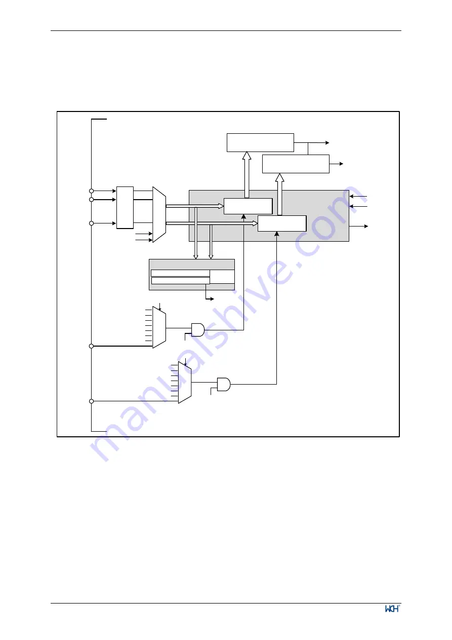
Figure 9-1 ADC module block diagram
TIM1_CH1
TIM1_TRGO
EXTSEL[2:0]
TIM1_CH2
TIM2_TRGO
TIM2_CH1
TIM2_CH2
SWSTART
TIM1_CH4
TIM1_CH3
JEXTSEL[2:0]
TIM2_CH3
TIM2_CH4
JSWSTART
EXTTRIG
GPIO
Port
Vref
Vcal
ADC_IN0
ADC_IN1
ADC_IN7
Rule channel
group
Injection
channel group
JEXTTRIG
Rule channel data
register (16 bits)
Injection channel data
register (4
×
16 bits)
Analog to
Digital
Converters
ADC_SAMPT
Rx
ADCCLK
Max=24MHz
DMA
Request
-ADC_IOFRx[9:0]
Analog Watchdog
High threshold (10-bit)
Low threshold (10-bit)
Compare
Results
JEOC=1
EOC=1
AWD=1
Conversion ends
End of Injection conversion
PD3/PC2
PD1/PA2
9.2.2 ADC configuration
1)
Module power-up
An ADON bit of 1 in the ADC_CTLR2 register indicates that the ADC module is powered up. When the ADC
module enters the power-up state (ADON=1) from the power-down mode (ADON=0), a delay period t
STAB
is
required for the module stabilization time. After that, the ADON bit is written to 1 again and is used as the
start signal for software to start the ADC conversion. By clearing the ADON bit to 0, the current conversion
can be terminated and the ADC module placed in power-down mode, a state in which the ADC consumes
almost no power.
2)
Sampling clock
The register operation of the module is based on the AHBCLK (AHB bus) clock, and the clock reference of
its conversion unit, ADCCLK, is configured by the ADCPRE field of the RCC_CFGR0 register to divide the
frequency, which cannot exceed a maximum of 24MHz.


