Page 142
13. 10-bit AD Converter (ADC)
13.2 Register configuration
TMP86PM29BUG
13.2 Register configuration
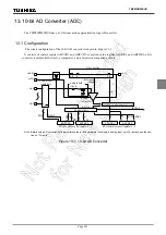
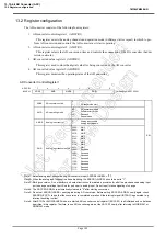
The AD converter consists of the following four registers:
1. AD converter control register 1 (ADCCR1)
This register selects the analog channels and operation mode (Software start or repeat) in which to per-
form AD conversion and controls the AD converter as it starts operating.
2. AD converter control register 2 (ADCCR2)
This register selects the AD conversion time and controls the connection of the DA converter (Ladder
resistor network).
3. AD converted value register 1 (ADCDR1)
This register used to store the digital value fter being converted by the AD converter.
4. AD converted value register 2 (ADCDR2)
This register monitors the operating status of the AD converter.
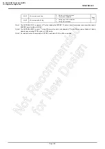
Note 1: Select analog input channel during AD converter stops (ADCDR2<ADBF> = "0").
Note 2: When the analog input channel is all use disabling, the ADCCR1<AINDS> should be set to "1".
Note 3: During conversion, Do not perform port output instruction to maintain a precision for all of the pins because analog input
port use as general input port. And for port near to analog input, Do not input intense signaling of change.
Note 4: The ADCCR1<ADRS> is automatically cleared to "0" after starting conversion.
Note 5: Do not set ADCCR1<ADRS> newly again during AD conversion. Before setting ADCCR1<ADRS> newly again, check
ADCDR2<EOCF> to see that the conversion is completed or wait until the interrupt signal (INTADC) is generated (e.g.,
interrupt handling routine).
Note 6: After STOP or SLOW/SLEEP mode are started, AD converter control register1 (ADCCR1) is all initialized and no data can
be written in this register. Therfore, to use AD converter again, set the ADCCR1 newly after returning to NORMAL1 or
NORMAL2 mode.
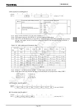
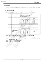
AD Converter Control Register 1
ADCCR1
(000EH)
7
6
5
4
3
2
1
0
ADRS
AMD
AINDS
SAIN
(Initial value: 0001 0000)
ADRS
AD conversion start
0:
1:
-
AD conversion start
R/W
AMD
AD operating mode
00:
01:
10:
11:
AD operation disable
Software start mode
Reserved
Repeat mode
AINDS
Analog input control
0:
1:
Analog input enable
Analog input disable
SAIN
Analog input channel select
0000:
0001:
0010:
0011:
0100:
0101:
0110:
0111:
1000:
1001:
1010:
1011:
1100:
1101:
1110:
1111:
AIN0
AIN1
AIN2
AIN3
AIN4
AIN5
AIN6
AIN7
Reserved
Reserved
Reserved
Reserved
Reserved
Reserved
Reserved
Reserved
Summary of Contents for TLCS-870/C Series
Page 1: ...8 Bit Microcontroller TLCS 870 C Series TMP86PM29BUG ...
Page 6: ...TMP86PM29BUG ...
Page 7: ...Revision History Date Revision 2007 10 11 1 First Release 2008 8 29 2 Contents Revised ...
Page 9: ......
Page 15: ...vi ...
Page 19: ...Page 4 1 3 Block Diagram TMP86PM29BUG 1 3 Block Diagram Figure 1 2 Block Diagram ...
Page 23: ...Page 8 1 4 Pin Names and Functions TMP86PM29BUG ...
Page 48: ...Page 33 TMP86PM29BUG ...
Page 49: ...Page 34 2 Operational Description 2 3 Reset Circuit TMP86PM29BUG ...
Page 61: ...Page 46 3 Interrupt Control Circuit 3 8 External Interrupts TMP86PM29BUG ...
Page 81: ...Page 66 6 Watchdog Timer WDT 6 3 Address Trap TMP86PM29BUG ...
Page 135: ...Page 120 10 8 Bit TimerCounter TC5 TC6 10 1 Configuration TMP86PM29BUG ...
Page 145: ...Page 130 11 Asynchronous Serial interface UART 11 9 Status Flag TMP86PM29BUG ...
Page 165: ...Page 150 13 10 bit AD Converter ADC 13 6 Precautions about AD Converter TMP86PM29BUG ...
Page 183: ...Page 168 15 LCD Driver 15 4 Control Method of LCD Driver TMP86PM29BUG ...
Page 201: ...Page 186 18 Electrical Characteristics 18 9 Handling Precaution TMP86PM29BUG ...
Page 203: ...Page 188 19 Package Dimensions TMP86PM29BUG ...
Page 205: ......

