Page 122
11. Asynchronous Serial interface (UART )
11.2 Control
TMP86PM29BUG
11.2 Control
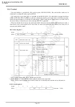
UART is controlled by the UART Control Registers (UARTCR1, UARTCR2). The operating status can be moni-
tored using the UART status register (UARTSR).
Note 1: When operations are disabled by setting TXE and RXE bit to “0”, the setting becomes valid when data transmit or receive
complete. When the transmit data is stored in the transmit data buffer, the data are not transmitted. Even if data transmit is
enabled, until new data are written to the transmit data buffer, the current data are not transmitted.
Note 2: The transmit clock and the parity are common to transmit and receive.
Note 3: UARTCR1<RXE> and UARTCR1<TXE> should be set to “0” before UARTCR1<BRG> is changed.
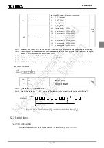
Note: When UARTCR2<RXDNC> = “01”, pulses longer than 96/fc [s] are always regarded as signals; when UARTCR2<RXDNC>
= “10”, longer than 192/fc [s]; and when UARTCR2<RXDNC> = “11”, longer than 384/fc [s].
UART Control Register1
UARTCR1
(0025H)
7
6
5
4
3
2
1
0
TXE
RXE
STBT
EVEN
PE
BRG
(Initial value: 0000 0000)
TXE
Transfer operation
0:
1:
Disable
Enable
Write
only
RXE
Receive operation
0:
1:
Disable
Enable
STBT
Transmit stop bit length
0:
1:
1 bit
2 bits
EVEN
Even-numbered parity
0:
1:
Odd-numbered parity
Even-numbered parity
PE
Parity addition
0:
1:
No parity
Parity
BRG
Transmit clock select
000:
001:
010:
011:
100:
101:
110:
111:
fc/13 [Hz]
fc/26
fc/52
fc/104
fc/208
fc/416
TC5 ( Input INTTC5)
fc/96
UART Control Register2
UARTCR2
(0026H)
7
6
5
4
3
2
1
0
RXDNC
STOPBR
(Initial value: **** *000)
RXDNC
Selection of RXD input noise
rejection time
00:
01:
10:
11:
No noise rejection (Hysteresis input)
Rejects pulses shorter than 31/fc [s] as noise
Rejects pulses shorter than 63/fc [s] as noise
Rejects pulses shorter than 127/fc [s] as noise
Write
only
STOPBR
Receive stop bit length
0:
1:
1 bit
2 bits
Summary of Contents for TLCS-870/C Series
Page 1: ...8 Bit Microcontroller TLCS 870 C Series TMP86PM29BUG ...
Page 6: ...TMP86PM29BUG ...
Page 7: ...Revision History Date Revision 2007 10 11 1 First Release 2008 8 29 2 Contents Revised ...
Page 9: ......
Page 15: ...vi ...
Page 19: ...Page 4 1 3 Block Diagram TMP86PM29BUG 1 3 Block Diagram Figure 1 2 Block Diagram ...
Page 23: ...Page 8 1 4 Pin Names and Functions TMP86PM29BUG ...
Page 48: ...Page 33 TMP86PM29BUG ...
Page 49: ...Page 34 2 Operational Description 2 3 Reset Circuit TMP86PM29BUG ...
Page 61: ...Page 46 3 Interrupt Control Circuit 3 8 External Interrupts TMP86PM29BUG ...
Page 81: ...Page 66 6 Watchdog Timer WDT 6 3 Address Trap TMP86PM29BUG ...
Page 135: ...Page 120 10 8 Bit TimerCounter TC5 TC6 10 1 Configuration TMP86PM29BUG ...
Page 145: ...Page 130 11 Asynchronous Serial interface UART 11 9 Status Flag TMP86PM29BUG ...
Page 165: ...Page 150 13 10 bit AD Converter ADC 13 6 Precautions about AD Converter TMP86PM29BUG ...
Page 183: ...Page 168 15 LCD Driver 15 4 Control Method of LCD Driver TMP86PM29BUG ...
Page 201: ...Page 186 18 Electrical Characteristics 18 9 Handling Precaution TMP86PM29BUG ...
Page 203: ...Page 188 19 Package Dimensions TMP86PM29BUG ...
Page 205: ......

