Page 32
2. Operational Description
2.3 Reset Circuit
TMP86PM29BUG
2.3.2
Address trap reset
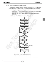
If the CPU should start looping for some cause such as noise and an attempt be made to fetch an instruction
from the on-chip RAM (when WDTCR1<ATAS> is set to “1”), DBR or the SFR area, address trap reset will be
generated. The reset time is maximum 24/fc[s] (1.5
µ
s at 16.0 MHz). Then, the
RESET
pin outputs "L" level
during maximum 24/fc[s].
Note:The operating mode under address trapped is alternative of reset or interrupt. The address trap area is alter-
native.
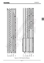
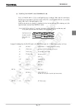
Note 1: Address “a” is in the SFR, DBR or on-chip RAM (WDTCR1<ATAS> = “1”) space.
Note 2: During reset release, reset vector “r” is read out, and an instruction at address “r” is fetched and decoded.
Note 3: Varies on account of external condition: voltage or capacitance
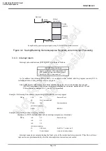
Figure 2-16 Address Trap Reset
2.3.3
Watchdog timer reset
Refer to Section “Watchdog Timer”.
2.3.4
System clock reset
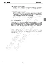
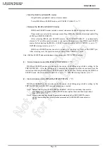
If the condition as follows is detected, the system clock reset occurs automatically to prevent dead lock of the
CPU. (The oscillation is continued without stopping.)
- In case of clearing SYSCR2<XEN> and SYSCR2<XTEN> simultaneously to
“
0
”
.
- In case of clearing SYSCR2<XEN> to
“
0
”
, when the SYSCR2<SYSCK> is
“
0
”
.
- In case of clearing SYSCR2<XTEN> to
“
0
”
, when the SYSCR2<SYSCK> is
“
1
”
.
The reset time is maximum 24/fc (1.5
µ
s at 16.0 MHz). Then, the
RESET
pin outputs "L" level during maxi-
mum 24/fc[s] (1.5
µ
s at 16.0MHz).
Instruction at address r
16/fc [s]
Maximum 24/fc [s]
Instruction
execution
Internal reset
signal
RESET output
JP a
Reset release
Address trap is occurred
("L" output)
4/fc to 12/fc [s]
Note 3
Summary of Contents for TLCS-870/C Series
Page 1: ...8 Bit Microcontroller TLCS 870 C Series TMP86PM29BUG ...
Page 6: ...TMP86PM29BUG ...
Page 7: ...Revision History Date Revision 2007 10 11 1 First Release 2008 8 29 2 Contents Revised ...
Page 9: ......
Page 15: ...vi ...
Page 19: ...Page 4 1 3 Block Diagram TMP86PM29BUG 1 3 Block Diagram Figure 1 2 Block Diagram ...
Page 23: ...Page 8 1 4 Pin Names and Functions TMP86PM29BUG ...
Page 48: ...Page 33 TMP86PM29BUG ...
Page 49: ...Page 34 2 Operational Description 2 3 Reset Circuit TMP86PM29BUG ...
Page 61: ...Page 46 3 Interrupt Control Circuit 3 8 External Interrupts TMP86PM29BUG ...
Page 81: ...Page 66 6 Watchdog Timer WDT 6 3 Address Trap TMP86PM29BUG ...
Page 135: ...Page 120 10 8 Bit TimerCounter TC5 TC6 10 1 Configuration TMP86PM29BUG ...
Page 145: ...Page 130 11 Asynchronous Serial interface UART 11 9 Status Flag TMP86PM29BUG ...
Page 165: ...Page 150 13 10 bit AD Converter ADC 13 6 Precautions about AD Converter TMP86PM29BUG ...
Page 183: ...Page 168 15 LCD Driver 15 4 Control Method of LCD Driver TMP86PM29BUG ...
Page 201: ...Page 186 18 Electrical Characteristics 18 9 Handling Precaution TMP86PM29BUG ...
Page 203: ...Page 188 19 Package Dimensions TMP86PM29BUG ...
Page 205: ......

