241
Chapter 8 A/D Converter
8
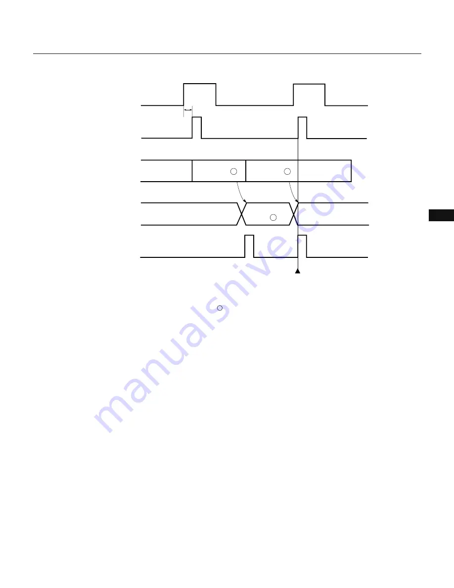
Fig. 8-14 Example of Malfunction in a Hardware-Started A/D Conversion
Notes 1.
When the operation is normal, the result of conversion 2 is stored. If a malfunction occurs, however, value 7FH is stored.
2.
Time from when an input to the INT5 pin changes to when its edge is asserted. See
Chapter 11
for details.
In order to solve this problem, the A/D converter mode register (ADM) must be set again after the necessary
A/D conversion is hardware-started and completed. A similar problem occurs during in-circuit emulation.
(6) When the result of A/D conversion is read by using a vectored interrupt during the scan mode, if the A/D
conversion end interrupt is kept pending for a prolonged time because of other interrupts being handled (at
least 180 clocks if the FR bit is 0 or 120 clocks if the FR bit is 1), the conversion result cannot be accurately
measured. To measure the conversion result accurately, take the following measures:
• Keep the time required to handle other interrupts adequately shorter than the required A/D conversion time.
• Use the multiplexed interrupt mode so that the A/D conversion end interrupt can be accepted even when
other interrupts are being handled.
• Use a macro service to handle the A/D conversion end interrupt.
Note that the A/D conversion end interrupt may also be kept pending by the causes described in Section 12.3.5.
Of the measures described above, the macro service might be the simplest method for you application.
(7) If the ADM register is set after registers related to interrupts have been set during the scan mode, an unwanted
interrupt may occur, thus causing the storage location of the conversion result to appear to have shifted. To
prevent this, take the actions listed below in the stated order.
• Write to the ADM register.
• Reset the interrupt request flag (PIF5) to 0.
• Set the interrupt mask flag or interrupt service mode flag.
ADCR
INTAD
Conversion trigger
INTP5
A/D converter
operatioon
Conversion completion and
conversion trigger occur
simultaneously
7FH
Note 1
Conversion 1
Conversion 2
Conversion
result 1
Note 2
Summary of Contents for PD78212
Page 11: ......
Page 53: ...24 ...
Page 61: ...32 µPD78214 Sub Series 9 VSS Ground 10 NC non connection Not connected inside the chip ...
Page 65: ...36 ...
Page 83: ...54 ...
Page 135: ...106 ...
Page 271: ...242 ...
Page 405: ...376 ...
Page 417: ...388 ...
Page 423: ...394 ...
Page 449: ...420 ...
Page 457: ...428 ...
Page 471: ...442 ...
Page 487: ...458 ...


