8XC196L
X SUPPLEMENT
8-14
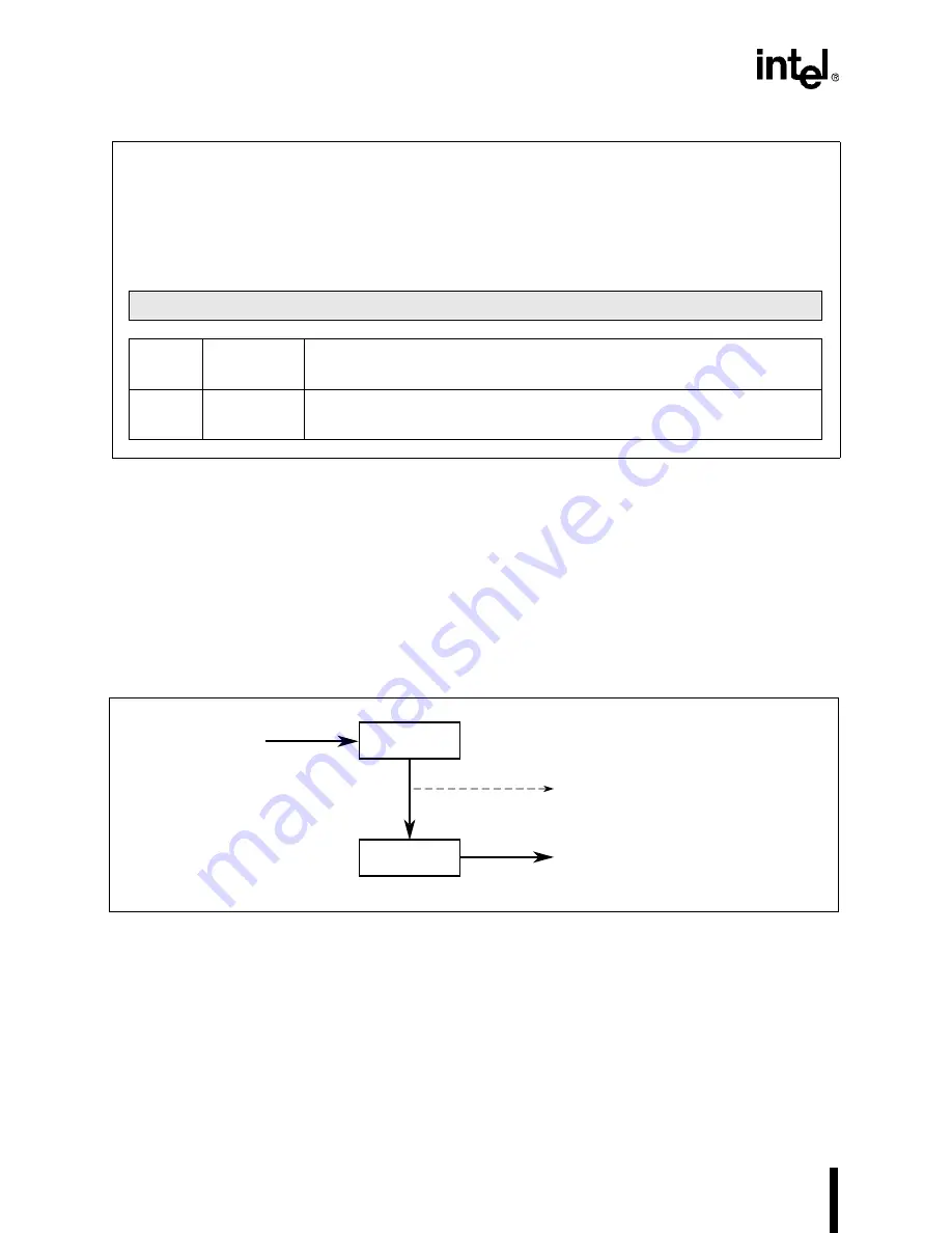
Transmitting the message requires that you first program the J1850 command (J_CMD) register
to specify the number of bytes you want to transfer across the J1850 bus. The number of bytes
specified must include the header byte(s). After the start of frame (SOF) symbol is put on the bus,
the first header byte is transferred to J_TX for transmission. This byte will automatically be trans-
ferred into the J1850 transmit buffer (JTX_BUF) and the second byte of the message frame will
be written to J_TX. The transfer of the first byte to JTX_BUF triggers the transmission process
and generates the J1850 transmission (J1850TX) interrupt (if it is enabled), signaling that J_TX
is available for another byte (Figure 8-13).
Figure 8-13. J1850 Transmit Message Structure
After the byte in JTX_BUF is transmitted, the byte residing in J_TX is automatically shifted into
JTX_BUF, freeing J_TX for another byte. This process continues until the CSM has resolved the
number of message bytes (MSG3:0) programmed into the J_CMD register.
If the last message byte being transmitted is shifted out before the MSGx count expires, a
J1850ST core interrupt is generated and the OVR_UNDR (J_STAT.3) bit records a transmitter
underflow error in the J_STAT register.
J_TX
Address:
Reset State:
1F50H
00H
The J1850 transmitter (J_TX) register transfers data in byte increments to the J1850 bus from the
microcontroller CPU. This register is buffered to allow for transmission of a second data byte while the
first data byte is being shifted out. This byte register can be read or written, and is addressable
through
windowing.
7
0
Transmit Byte
Bit
Number
Bit
Mnemonic
Function
7:0
DB7:0
Data Bits
These eight bits compose the data byte to be transmitted to the J1850 bus.
Figure 8-12. J1850 Transmitter (J_TX) Register
A5235-01
CPU
JTX_BUF
J_TX
Message transmit
interrupt (J1850TX) set
J1850 Bus
Summary of Contents for 87C196CA
Page 9: ...1 Guide to This Manual...
Page 10: ......
Page 13: ...2 Architectural Overview...
Page 14: ......
Page 22: ......
Page 23: ...3 Address Space...
Page 24: ......
Page 33: ...4 Standard and PTS Interrupts...
Page 34: ......
Page 43: ...5 I O Ports...
Page 44: ......
Page 51: ...6 Synchronous Serial I O Port...
Page 52: ......
Page 56: ......
Page 57: ...7 Event Processor Array...
Page 58: ......
Page 65: ...8 J1850 Communications Controller...
Page 66: ......
Page 89: ...9 Minimum Hardware Considerations...
Page 90: ......
Page 93: ...10 Special Operating Modes...
Page 94: ......
Page 98: ......
Page 99: ...11 Programming the Nonvolatile Memory...
Page 100: ......
Page 106: ......
Page 107: ...A Signal Descriptions...
Page 108: ......
Page 118: ......
Page 119: ...Glossary...
Page 120: ......
Page 133: ...Index...
Page 134: ......


