background image

IT3/IT5


Connector System       


PWB


A

SSEMBLY 

N

OTES


Document Number:


ETAD-F0458


Revision 3.10


Page 

40

 of 

73


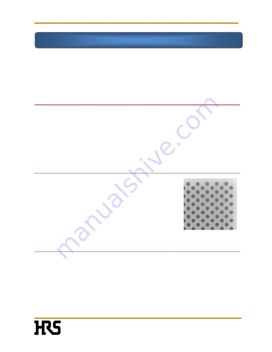
The Hirose IT3/IT5 receptacles’ 6mm or 7mm heights allow for high-resolution, low-noise x-ray 
imaging.  Whether a mounting  or mating  receptacle,  and  regardless of the  stacking  height  of 
the  final  assembly,  the  images  remain  consistent.    No  special  modifications  to  the  image 
analysis routine to compensate for different connector heights are needed. 

Unless specifically mentioned, IT3 and IT5 share the same capability and requirement. 

9.1 Sampling Frequency


100% of the components should be inspected

 for the following defect modes: 


Solder Bridges 


Cold Solder Joints 


Open Solder Joints 


Cracks 


Head-In- Pillow* 


Excessive Voids 

 
*  The 

appearance

  of 

head-in-pillow

  defects  in 

ball-on-pin 

BGA  constructions 

differs

  slightly 

from  their  typical  appearance  in 

ball-on-pad

  constructions.    Refer  to  section  11,  Tips  for  SMT 

Assembly for more information on head-in-pillow. 


9.2 X-Ray Laminography


As part of the production process, 3-dimensional x-ray 
laminography should be used to inspect the assembly after 
reflow processing.


If the automatic inspection system reports potential soldering 
defects, 

the defects should be verified

 by visual inspection 

and/or 2-dimensional transmission x-ray inspection with oblique 
angle views before beginning the rework procedure. 


9.3 Visual Inspection


 If  the  suspected  defect  is  near  the  outside  edge  of  the  receptacle,  it  may  be  visible  using 
optical  devices.  Visual  inspection  tools  include  devices  ranging  from  hand-held  mirrors  to 
digital endoscopes.  If the suspected defect is on an interior ball, it may require 2-dimensional 
x-ray for verification. 

Section 9 Inspection 

Nov.1.2022 Copyright 2022 HIROSE ELECTRIC CO., LTD. All Rights Reserved.

Summary of Contents for Hirose IT3

Page 1: ...F0458 Revision 3 10 Hirose IT3 IT5 Connector System GENERAL INFORMATION DESIGN NOTES PWB ASSEM BLY NOTES TIPS FOR SMT ASSEMBLY SYSTEM ASSEM BLY SYSTEM DISASSEMBLY Winner of 2009 SMT Vision Award Nov 1 2022 Copyright 2022 HIROSE ELECTRIC CO LTD All Rights Reserved ...

Page 2: ...r Direction 22 3 6 Alignment Tolerances 23 4 0 Introduction to Assembly 24 5 0 Stencil Printing 24 5 1 Solder Paste Selection 24 5 2 Stencil Design 25 5 3 Effect of Alignment 25 5 4 Paste Print Quality 26 6 0 Pick and Place 27 6 1 Packaging 27 6 2 Media Trays 28 6 3 Pre bake 29 6 4 Pick Point 29 6 5 Component Weight 30 6 6 Visionand Alignment 30 6 7 Placement Force 31 6 8 Orientation Indicator 31 ...

Page 3: ...10 3 Reflow Profile Considerations 44 10 4 Suggested Thermal Profiles 44 10 5 Special Profiling Considerations 45 10 6 Receptacle Removal 45 10 7 Site Redressing 46 10 8 Solder Replenishment 48 10 9 Receptacle Replacement 48 10 10 Reflow Soldering 49 10 11 Inspection 49 10 12 Rework Solder Paste Selection 49 11 0 Tips for SMT Assembly 51 11 1 Stencil Printing 51 11 2 Pickand Place 55 11 3 Reflow 5...

Page 4: ... press force information and other information with respect to design note release November 30 2009 1 55 Updated the front page and revised information on footprint December 30 2009 1 56 Updated reworkand packaging information December 13 2010 1 6 Updated height variation chart and interposer installation cap February 24 2011 2 0 Included information on plugs andan interposer removal tool May 1 20...

Page 5: ... bulletin is intended to provide basic information and product features of the Hirose IT3 IT5 BGA connector system By providing this information Hirose believes it can help its customers to speed product development improve quality and reliability and limit overall system costs 1 2 Scope This guideline provides information useful for applications using the IT3 IT5 BGA connector system It provides ...

Page 6: ...SCLAIMS ALL WARRANTIES EXPRESS OR IMPLIED INCLUDING BUT NOT LIMITED TO THE IMPLIED WARRANTIES OF MERCHANTABILITY AND FITNESS FOR A PARTICULAR PURPOSE HIROSE DOES NOT WARRANT THAT THE GUIDELINES CONTAINED IN THIS BULLETIN WILL MEET ANY CUSTOMER S REQUIREMENTS FURTHERMORE HIROSE DOES NOT WARRANT OR MAKE ANY REPRESENTATIONS REGARDING THE USE OR THE RESULTS OF THE USE OF INFORMATION CONTAINED IN THIS ...

Page 7: ...s are compatible with popular mezzanine connectors Receptacles are available in tin lead and lead free configurations for IT3 and lead free for IT5 They can be used in no clean or water wash assembly processes The interposer is an assembly consisting of individual wafers each carrying 10 signal and 9 ground connections for IT3 and 10 signal and 11 ground connections for IT5 The interposer is mount...

Page 8: ...gnals 90 grounds IT3M 100S BGA 2 5 g 200 200 signals 180 grounds IT3M 200S BGA 4 7 g 300 300 signals 270 grounds IT3M 300S BGA 9 1 g Contact Positions Part Number Weight 100 100 signals 110 grounds IT5D 100S BGA 2 7 g 200 200 signals 220 grounds IT5D 200S BGA 5 2 g 300 300 signals 330 grounds IT5D 300S BGA 9 9 g Receptacle will accept any available stacking height IT3 Mating Receptacle IT3 Mountin...

Page 9: ... 100 signals 110 grounds IT5M 100S BGA 2 7 g 200 200 signals 220 grounds IT5M 200S BGA 5 2 g 300 300 signals 330 grounds IT5M 300S BGA 9 9 g Receptacle will accept any available stacking height Contact Positions Part Number Weight 100 100 signals 110 grounds IT5HM 100S BGA 3 5 g 200 200 signals 220 grounds IT5HM 200S BGA 6 7 g 300 300 signals 330 grounds IT5HM 300S BGA 12 8 g Receptacle will accep...

Page 10: ...age 6 of 73 Components listed in gray letters are under development IT3 IT5 Interposer IT3 IT5 100P 38H IT3 IT5 200P 38H IT3 IT5 300P 38H IT3 IT5 100P 18H IT3 IT5 200P 18H IT3 IT5 300P 18H IT3 Interposer Height Variation Nov 1 2022 Copyright 2022 HIROSE ELECTRIC CO LTD All Rights Reserved ...

Page 11: ...umber ETAD F0458 Revision 3 10 Page 7 of 73 IT5 Interposer Height Variation Components listed in gray letters are under development IT3 Plug IT3M 100P 15BGA IT3M 200P 15BGA IT3M 300P 15BGA Nov 1 2022 Copyright 2022 HIROSE ELECTRIC CO LTD All Rights Reserved ...

Page 12: ...ign is different its outlines defined in white for emphasis IT3 receptacles have latches on sides while IT5 s do not The difference between IT3 and IT5 interposers is that on IT5 interposer a label is adhered on a shorter side away from the polarity chamfer to indicate Hirose part number and other information Polarity chamfer Label exclusive to IT5 interposer Nov 1 2022 Copyright 2022 HIROSE ELECT...

Page 13: ...eptacle customized IT5HM xxxS BGA 1mm Mounting Receptacle IT5HMx xxxS BGA 1mm Mounting Receptacle customized IT3M xxxP xxBGA Plug IT3Mx xxxP xxBGA Plug customized 3 Contact Positions 100 200 300 4 Connector S Socket P Plug 5 BGA Ball Grid Array No further designation 6 Package Specification Blank Standard xx Customized 7 Material and Plating Specification of Receptacle and Plug 37 Pb free Solder S...

Page 14: ...housing color gray 8 Interposer type Blank Standard xx Customized 9 Stacking Height mm 14 15 17 18 20 22 25 26 28 30 32 35 38 40 10 Plating Specification of Interposer 03 Contact Area Gold 0 76 μm Ni 1 5 μm Customized IT3 interposers cannot mate with standard IT5 receptacles 2 4 Manufacturing Lot Number These configurations are the same with IT3 and IT5 connector parts Lot number indication may be...

Page 15: ...s 100 200 300 No of Ground Contacts IT3 IT5 90 110 180 220 270 330 A Receptacle Length 21 38 5 56 B Receptacle Width 19 2 19 2 19 2 C1 Regular Receptacle Height 6 6 6 C2 1mm Receptacle Height 7 7 7 D Interposer Plug Outline Length 24 41 5 59 E Interposer Plug Outline Width 21 21 21 All dimensions shown are in mm C2 Interposer and Plug Outlines Shown 200 position mounting receptacle IT3M 200S BGA S...

Page 16: ...nted to the board as a lightweight receptacle and an interposer is used to connect to parallel PWBs at many different height options Standoffs must be used in conjunction with the interposers to help reinforce the structure of the final multi PWB assembly Unless specificallymentioned IT3 and IT5 share the same capability and requirement Mating Receptacle Interposer Mounting Receptacle Section 3 PW...

Page 17: ...fined or metal defined pads are recommended Recommended sizes and clearances are shown below All dimensions shown are in mm Through via sizes will depend on PWB thickness and fabricator s capabilities Vias should be placed far enough from the pad to ensure a minimum solder dam width of 0 13mm Circular openings in the solder mask are preferred but D shape openings are acceptable if the minimum spac...

Page 18: ... diameter of the pad to compensate for typical variations in the assemblyprocess The specified clearance or solder mask relief from the copper feature is 0 05mm Precaution Verify fabricator capability Solder mask registration must be accurate to at least 0 05mm PWB fabricator s registration capability should be verified Depending on thickness of PWB fabricator s aspect ratio capabilities for throu...

Page 19: ...ent Number ETAD F0458 Revision 3 10 Page 15 of 73 Mating Receptacle IT3 D Mounting Receptacle IT5 H M IT3 D S BGA Footprint IT5 M S BGA Footprint All dimensions shown are in mm Nov 1 2022 Copyright 2022 HIROSE ELECTRIC CO LTD All Rights Reserved ...

Page 20: ...75 B 28 10 45 60 63 10 C 30 10 47 60 65 10 The differences between IT3 and IT5 footprints are 1 IT5 footprint has additional ground rows Xand Y 2 IT5 footprint has narrower vertical minimum clearance for all devices and forsensitive devices All dimensions shown are in mm IT5 D S BGA Footprint Nov 1 2022 Copyright 2022 HIROSE ELECTRIC CO LTD All Rights Reserved ...

Page 21: ...er with the chamfer is nearest to pin A1 Annotation For visual inspection purposes Pin 1 should be denoted on the silkscreen of the PWB bya specific marking e g asterisk or other accepted symbol near the A1 contact location and chamfer Mating Receptacle Interposer Mounting Receptacle Polarity chamfer Polarity chamfer Polarity chamfer IT3 D S BGA IT3 M S BGA Nov 1 2022 Copyright 2022 HIROSE ELECTRI...

Page 22: ...mbination with other IT3 IT5 connectors If multiple connectors are used on the same PWB they must be oriented in the same direction as shown below It is not recommended to mix orientations It is not recommended to multiple mate with IT3 plugs for 2 piece solution Correct Orientations Do not mix orientations Nov 1 2022 Copyright 2022 HIROSE ELECTRIC CO LTD All Rights Reserved ...

Page 23: ...male male M3 thread 3 3 Spacers Spacers are required to support the PWB s and protect the BGA solder joints Suggested spacer style is shown at lower right The recommended spacer height corresponds to the interposer stacking heightas shownin the chart below Nov 1 2022 Copyright 2022 HIROSE ELECTRIC CO LTD All Rights Reserved ...

Page 24: ...s 24 10 209 20 If overlap distance is more than half the length of the connector Interposer Outline Connector Pitch Two spacers located diagonally are minimally required Some applications may require four spacers Spacers should be located 10 50 mm from the corners of the receptacles to prevent excessive mechanical loading on the interconnections If assembly will be subjected to vibration spacers s...

Page 25: ... purposes of disassembly and field replacement Tandem Mounting Socket Combinations Connector Minimum Pitch mm Connector Maximum Pitch mm IT3 IT5 100pos IT3 IT5 100pos 26 05 211 00 IT3 IT5 200pos IT3 IT5 200 pos 43 55 228 50 IT3 IT5 300pos IT3 IT5 300 pos 61 05 246 00 IT3 IT5 100pos IT3 IT5 200 pos 34 80 219 75 IT3 IT5 100pos IT3 IT5 300 pos 43 55 228 50 IT3 IT5 200pos IT3 IT5 300 pos 52 30 237 25 ...

Page 26: ...irection Do not mix mating and mounting receptacles on the same PWB All interposers must engage in the same direction as shown below Correct Method all connectors mate in same direction Incorrect Method connectors mate in different directions Nov 1 2022 Copyright 2022 HIROSE ELECTRIC CO LTD All Rights Reserved ...

Page 27: ...roper mating fits in cases of multiple connectors All dimensions shownare in mm Mating tolerances Due toits 3 piece design the IT3 IT5 connector system can accept mating tolerances of up to 0 3mm tolerance in the X axis and up to 0 2mmin the Y axis All dimensions shown are in mm X 0 05 Y 0 05 Global fiducial 0 3 0 2 X Axis Y Axis Nov 1 2022 Copyright 2022 HIROSE ELECTRIC CO LTD All Rights Reserved...

Page 28: ... the same capability and requirement The Hirose IT3 IT5 BGA connector has print characteristics similar to 1 0mm BGA device Its pads are 0 6mm diameter on a staggered 1 5 x 1 75mm grid It requires no special aperture designs or stencil thicknesses and can be successfully printed in any process that is capable of printing 1 0mm BGA s Unless specifically mentioned IT3 and IT5 share the same capabili...

Page 29: ... 0 54mm square apertures may also be used if so their corners should have radius of at least 0 1mm 5 3 Effect of Alignment Stencil thicknesses of 125 to 150 microns are best thicknesses of 100 124 microns and 151 175 microns are acceptable Thicknesses less than 100 microns or greater than 175 microns are not recommended ALIGNMENT MISALIGNMENT GOOD PRINT ACCEPTABLE PRINT Circular apertures more rob...

Page 30: ... deposits should be of uniform size and shape with good definition Excess flux or paste between the pads is not acceptable Solder Paste Print Comparison Precautions Solder paste print quality is a very important factor in achieving a high quality assembly process If preferred or acceptable print quality is not obtained refer to section 11 Tips for SMT Assembly Preferred Acceptable Unacceptable Nov...

Page 31: ...acle trays will be sealed inside a bag with deoxidizing agent and desiccant Please do not mount these receptacles after 4 weeks of opening the bags according to J STD 0208 MSL2A in IPC JEDEC standards Receptacles comply with JEDEC standards JEDEC PUBLICATION 95 DESIGN GUIDE 4 10 The expiration time for receptacles within close bags is 12 months or one year from the delivery date when the effect of...

Page 32: ...rays IT3 IT5 receptacle components are shipped with pick and place tape attached in JEDEC hard trays as shown below JEDEC Tray for IT3 IT5 100 Position Receptacles JEDEC Tray for IT3 IT5 200 Position Receptacles All dimensions shown are in mm Nov 1 2022 Copyright 2022 HIROSE ELECTRIC CO LTD All Rights Reserved ...

Page 33: ...6 3 Pre bake The connector body materials do not absorb water from the atmosphere therefore pre bake is not required for IT3 and IT5 receptacles 6 4 Pick Point Pick locations and dimensions for IT3 and IT5 receptacles are shown below Pick points are located at the geometric centers of receptacles Removable metal cap on 300 pos receptacle 17 20 3 Tape Removal 17 16 3 Tape Removal 13 5 Φ15 Φ10 Φ15 N...

Page 34: ...erial Weight 100 IT3M D 100S BGA 37 39 Pb free SAC 305 solder 2 5 g IT3M D 100S BGA 57 Eutectic SnPb solder IT5M D 100S BGA 37 39 Pb free SAC 305 solder 2 7 g IT5HM HD 100S BGA 37 39 Pb free SAC 305 solder 3 5 g 200 IT3M D 200S BGA 37 39 Pb free SAC 305 solder 4 7 g IT3M D 200S BGA 57 Eutectic SnPb solder IT5M D 200S BGA 37 39 Pb free SAC 305 solder 5 2 g IT5HM HD 200S BGA 37 39 Pb free SAC 305 so...

Page 35: ...lts balls should be approximately to the depth of the solder paste Consult placement equipment manufacturer for specific guidelines regarding BGA mounting 6 8 Orientation Indicator The receptacle s polarity is indicated by a chamfer on one corner as shown below Mating Receptacle Mounting Receptacle Polarity chamfer Polarity chamfer IT3 D S BGA IT3 M S BGA IT3M S BGA IT3D S BGA Nov 1 2022 Copyright...

Page 36: ...less specifically mentioned IT3 and IT5 share the same capability and requirement 7 1 Instrumentation The reflow process should be recorded using a digital data logger with thermocouples attached to key locations on the PWB and connector 7 2 Thermocouple Attachment A minimum of two thermocouples should be used on the IT3 IT5 connector receptacle One should be located on an inside ball preferably a...

Page 37: ...t with paste manufacturer for optimum profile settings 7 5 Other Important Factors Check thermal exposure limits of PWB laminate if processing with lead free solder Time typically 3 to 7 minutes total SnPb Temperatures 0 C 250 217 230 240 183 205 225 Reflow Profile SnAgCu Temperatures 0 C 260 21 21 Max Body Temp Max Peak Temp Min Peak Temp Melting Point Reflow Min Soak Temp 140 160 Nov 1 2022 Copy...

Page 38: ...ll and they have been successfully assembled in inverted positions in production environments While the IT3 plugs are also compatible with the double sided reflow soldering please be cautious of the inverted reflow soldering with the plugs Thermoset plastic can be used to bond the standoffs of a plug to a PCB thus creating extra adhesion to prevent the plug from potentially falling out during the ...

Page 39: ...vailable Contact Hirose for more information 7 10 Cap Removal The metal cap is secured onto the 300 pos receptacle with four small latches that are located on either side of the lifting tabs To remove the cap hold it by its removal tabs Cap Cap Latches Tab to lift a cap IT3 series receptacle Cap latches Nov 1 2022 Copyright 2022 HIROSE ELECTRIC CO LTD All Rights Reserved ...

Page 40: ...g the other side in place Precaution It is important to roll the cap off the connector gently It is designed to separate very easily with this method Pushing the latch into the connector will not cause separation and may damage the connector body and or solder joints Nov 1 2022 Copyright 2022 HIROSE ELECTRIC CO LTD All Rights Reserved ...

Page 41: ...tures 60 650 C Cleaning time is a function of belt speed for in line cleaning machines and can be set manually for most batch cleaners Agitation is the mechanical scrubbing action of the water and can be controlled by changing the flow rate pressure number of nozzles or angle of the water delivery system depending on the type of cleaning machine used For most BGA devices a shallow impingement angl...

Page 42: ...vironment 8 3 No Clean Solder Process No Clean solder pastes are designed to be left on the circuit board If reflowed properly the residues will not interfere with circuit function Many no clean fluxes contain rosin which is not water soluble If cleaning of no clean flux residue is desired cleaning agents must be used Contact solder paste supplier for compatible cleaning agents and appropriate con...

Page 43: ... the entire surface of the PWB and is typically used as a process indicator to monitor cleaning processes in production environments Ion chromatography measures localized ionic contamination in specific areas of the PWB and is typically used during development efforts to verify the cleanability of a soldering product the effectiveness of a cleaning agent or process compatibility of a new component...

Page 44: ... constructions differs slightly from their typical appearance in ball on pad constructions Refer to section 11 Tips for SMT Assembly for more information on head in pillow 9 2 X Ray Laminography As part of the production process 3 dimensional x ray laminography should be used to inspect the assembly after reflow processing If the automatic inspection system reports potential soldering defects the ...

Page 45: ...tation for BGA s Note that the connector design is ball on pin style If pins appear as voids during x ray analysis parameters should be adjusted to eliminate the false detection of voids 9 5 Transmission 2 Dimensional X Ray A 2 dimensional x ray system can be used to verify certain defects that are indicated by the 3 dimensional inspection particularly if the interconnections are viewed at oblique...

Page 46: ...routines Solder Defect Detected via 3D X ray Inspection Solder Defect Verified via 2D X ray Inspection Defect Perform BGA Rework Optical Inspection Using Hand held Mirrors or Endoscope Inspect Solder Joint Attachment via 2D X ray Tighten Acceptance Threshold on 3D X ray Re inspect solder joints via 3D X ray No Yes Nov 1 2022 Copyright 2022 HIROSE ELECTRIC CO LTD All Rights Reserved ...

Page 47: ...lease remove the interposer for such rework Interposer removal procedure is on page 73 Unless specifically mentioned IT3 and IT5 share the same capability and requirement 10 1 Equipment and Supplies Forced Hot Air BGA Repair Station with bottom side heaters properly sized custom nozzle vacuum pickup low placement force capability and split vision alignment system Adhesive polyimide tape discs 3 8 ...

Page 48: ... be used to prevent PWB damage Removal and reattachment profiles should follow same guidelines as mass reflow process 10 4 Suggested Thermal Profile Ranges Time typically 3 to 7 minutes total SnPb Temperatures 0 C 250 217 230 240 183 205 225 Reflow Profile SnAgCu Temperatures 0 C 260 21 21 Max Body Temp Max Peak Temp Min Peak Temp Melting Point Reflow Min Soak Temp 140 160 Nov 1 2022 Copyright 202...

Page 49: ...posure in these areas The tape or cap should not be peeled off the receptacle prior to reflowing the solder joints 2 Component body should not be cooled during reflow heating Some convection rework systems offer the option of component body cooling during the rework process This should not be used on the IT3 IT5 connector Its open body design allows good heat transfer and low delta T s between sol...

Page 50: ...reheated to 150o C if tin lead solder is used and 180o C if lead free solder is used Soldering irons and wick should not be used to remove excess solder This method provides the highest risk of lifted pads torn traces or damaged solder mask If wick must be used to remove the excess solder see section titled Solder Wicking Guidelines on next page Vacuum Solder Removal Guidelines Liquid flux should ...

Page 51: ...older should remain on the pads to help prevent exposure of the intermetallic compound IMC layer to the atmosphere which can allow it to oxidize An oxidized IMC layer is less solderable than a properly redressed pad and could result in an open interconnection after the repair Inspection After solder removal the site should be thoroughly cleaned and dried before continuing At this time the pads and...

Page 52: ...ignment between the stencil apertures and the pads is critical Some BGA rework procedures include printing paste on the balls of the BGA Due to the compliant nature of the ball on pin design of the IT3 IT5 connector printing paste directly on the BGA balls is not recommended Precautions Solder MUST be applied to the pads during the rework process Use of flux alone has been shown to result in reduc...

Page 53: ...e appearance as non reworked solder joints If no defects are noted during visual inspection it should then be evaluated by 2 dimensional x ray If no defects are noted under the 2 D x ray inspection rework can be considered successful 10 12 Rework Solder Paste Selection Precautions The type of solder paste used in rework should be selected carefully The alloy tin lead or lead free should be verifie...

Page 54: ...water soluble solder paste may be used for the repair If the assembly has already been washed and sensitive components have been added no clean paste may be required Oringial Paste Type Cleaned Rework Paste Type Clean After Rework No Clean No No Clean No No Clean Yes No Clean Yes Water Soluble No Water Soluble Yes Water Soluble Yes No Clean No Nov 1 2022 Copyright 2022 HIROSE ELECTRIC CO LTD All R...

Page 55: ...t is on the stencil the diameter of the bead should be approximately 1 5cm Watch it during the print stroke It should roll over the surface of the stencil and should release cleanly from the squeegee blade when the blade lifts away from the stencil If the paste does not show this desired behavior remove it from the stencil and replace it with freshsolder paste 2 Remove the stencil from the printer...

Page 56: ...ptimums Squeegee pressure too high Decrease pressure It should be justenough to geta clean wipe across topsurface of stencil Too much paste on stencil Check paste bead on stencil 1 1 5cm diameter is typical Paste is too warm Check paste temperature and consult paste manufacturer s recommendations Print Definition is considered good if all deposits are of uniform shape and size with well defined ed...

Page 57: ...ee pressure too low Adjust pressure Itshould be justenough to get a clean wipe across top surface of stencil Not enough paste on stencil Check paste bead on stencil 1 1 5cm diameter is typical Paste is too cold Check paste temperature and consult paste manufacturer s recommendations Paste sticking to squeegee Check paste bead on stencil 1 1 5cm diameter is typical Check paste temperature Squeegee ...

Page 58: ...t air leveling Labels inks or other surface features create a gap between stencil and PWB If defects occur nearsurface features consider changing placement of those features or half etch stencil from underside toallow clearance for feature Bad Alignment An alignment error of up to 50 microns is typical and usually acceptable depending on tolerances in other parts of the assembly process If alignme...

Page 59: ...s placing connector receptacle more than 0 1mm off pad investigate the root cause Misplacement Possible Cause Suggested Action Poor vision capture miscalculated centroid Check vision inspection system Make sure to inspect all balls not just corner balls Wrong Orientation See section on orientation below Componentshifting on nozzle Check nozzle for obstructions make sure nozzle size is appropriate ...

Page 60: ... when two or more adjacent conductors are connected bysolder Solder Shorts Possible Cause Suggested Action Poor solder paste print Check paste print quality Placement pressure is too high and deforms solder paste deposit Check placement pressure and depth of placement Reflow profile taking toolong to reach liquidus temperature causing hot slumpand or and exhausting the flux Shorten time to reachli...

Page 61: ...reflow oven The sphere material and solder deposit do not fuse together to become one contiguous mass Typically the reason they do not fuse together is because one or both of the molten masses are covered with a thin but tough film of oxide that prevents them from mingling with each other This oxide film is often formed in the reflow process by one or more contributing factors Note that the HIP de...

Page 62: ...rface Contact PWB supplier Solder in Vias If solder is detected in a via it has likely been taken from a neighboring joint leaving that joint with insufficient solder Solder in Via Possible Cause Suggested Action Poor solder paste print Check paste print quality Damaged solder mask dam Inspect mask between pads and vias for flaking or other signs of poor adhesion 11 4 X Ray Inspection False Calls ...

Page 63: ...w If the pins are being detected as voids during x ray inspection modify the inspection routine to eliminate the false failure HIP defects may be detected as shorts because the condition forces the ball s image outside of the normally recognized ball area of the x ray program If images are captured that show offsets similar to the one above check for head in pillow defect Nov 1 2022 Copyright 2022...

Page 64: ...or sufficient volumes good definition and alignment with pads Opens Opens are often the result of insufficient solder paste deposits Following the printing process described above Make sure all apertures are completelyfilled before removing the tape from the stencil After removing the stencil from the PWB check the apertures to make sure the paste released If paste does not release well check its ...

Page 65: ... to peak temperature of thermal profile Keep delta Tacross component under 10 degrees Package warpage Shorten time toliquidus of thermal profile Ensure parts are dry Poor solder paste fusion Shorten time toliquidus of thermal profile Use nitrogenas reflow medium Head In Pillow Shorten time toliquidus of thermal profile Ensure balls are not contaminated or oxidized Nearby components affected Ifseco...

Page 66: ...tures For high assembly volumes dedicated tooling is suggested to ensure quality and ease of operation Unless specificallymentioned IT3 and IT5 share the same capability and requirement 12 1 Interposer Installation The interposersnaps on to the mounting receptacle as shown below The snap fit is achieved bya locking latch on each end of the interposer Locking Latch Section 12 System Level Assembly ...

Page 67: ...poser and pressedonas shown below Precaution It is very important to provide good underside board support wheninstalling the interposers A simple tooling plate can be fabricated to support the PWB and prevent it from flexing when the interposers are installed Interposer Polaritychamfer Polarity chamfer Mating Receptacle Nov 1 2022 Copyright 2022 HIROSE ELECTRIC CO LTD All Rights Reserved ...

Page 68: ...rposer should slide easily onto the mounting receptacle Place an installation cap The side with horizontal grooves should face up Push vertically down to engage the locking latches through an installation cap After the interposer is mounted install spacers onto motherboard notshown To install mating receptacle align the spacer holes in the daughter card with the threads on the spacers Press firml ...

Page 69: ...he assembly to lock the mating receptacle in place Install nuts onto the spacer threads Tighten nuts to specified torque 12 3 Installation Cap The installation cap is recommended to ensure qualityandease of operation during interposer installation Caps are reusable but should be discarded if theyshow signs of damage or wear Theyshould be stored properly when notin use and kept clean of dust and de...

Page 70: ...xturing system is suggested Board to Board Assembly Fixturing Insert spacer nuts into nests in assembly fixture Place motherboard on fixture Align guide pins with PWB tooling holes Assure motherboard sits flat on fixture Place interposers on top of mounting receptacles Align interposers and receptacles by their chamfered corners Nov 1 2022 Copyright 2022 HIROSE ELECTRIC CO LTD All Rights Reserved ...

Page 71: ...ith new cap Use top press plate to push directly down on interposers and lock them into place Press forceshould not exceed 500N for 300 pos 400N for 200 pos and 300N for 100 pos If a mechanical press is used force must be measureableand controlled Example One 200 signal connector do not exceed 400N insertion force Two 200 signal connectors 400 signals do not exceed 800N insertion force Nov 1 2022 ...

Page 72: ... process to protect wafers from dropped fasteners or tools Precaution It is veryimportant to tighten nuts to torque specified by OEM Failure to follow designers recommendations can result insystem damage or decreased reliability Position daughtercard over motherboard Usespacer studs for initial alignments When mating receptacles arealigned with interposers board will drop into place Nov 1 2022 Cop...

Page 73: ...uld not exceed 500N for 300 pos 400N for 200 pos and 300N for 100 pos Example One 200 signal connector do not exceed 400N insertion force Two 200 signal connectors 400 signals do not exceed 800N insertion force Install nuts on spacer studs Tighten to specified torque Assembly mating process is now complete Nov 1 2022 Copyright 2022 HIROSE ELECTRIC CO LTD All Rights Reserved ...

Page 74: ...cuit boards or interposers can result in permanent damage to the circuit assemblies Unless specificallymentioned IT3 and IT5 share the same capability and requirement 13 1 Daughter Card Removal To remove a daughter card first remove the nuts from the reinforcing spacers then lift the daughter cardstraight off the interposers as shown Precaution It is very important to prevent excessive flexing of ...

Page 75: ... possible without contacting any components On denselypopulated assemblies the edges maybe the only open area that can be grasped 13 2 Interposer Removal The IT3 interposer is secured onto the mounting receptacle with snap fit tabs shown below The IT3 interposeris secured onto the mounting receptacle also with other snap fit tabs shown below The IT5 interposer uses this mechanism solely Locking La...

Page 76: ...hout IT3 locking latches 2 Gently rotate one side of the Interposer Assembly laterally 10 o maximum Caution do not rotate more than 10 degrees 3 While gently rotating pull up on other side of the Interposer Assembly 4 The Interposer Assembly is removed from the board assembly and the Mounting Receptacle is ready to accept another Interposer Assembly Grasp by sides Locking Latch Locking Latch 10o M...

Page 77: ...val tool 2 Gently rotate one side of the Interposer Assembly laterally 10 o maximum using the tool Caution do not rotate more than 10 degrees 3 While gently rotating pull up on other side of the tool 4 The Interposer Assembly is removed as it is inside the tool Precaution Visuallyinspect the interposer before reinstalling it Discard if it shows anysigns of damage or wear Do notsubjectinterposer as...

Page 78: ...HIROSE ELECTRIC U S A INC High Speed Interconnects 3255 Scott Blvd Building 7 Ste 101 Santa Clara CA 95054 U S A www hiroseusa com Nov 1 2022 Copyright 2022 HIROSE ELECTRIC CO LTD All Rights Reserved ...

Reviews: