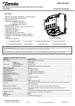
CY8C28xxx PSoC Programmable System-on-Chip TRM, Document No. 001-52594 Rev. *G
375
Digital Blocks
Figure 17-30. Typical SPIS Timing in Modes 2 and 3
Slave Select (SS_, active low).
Slave Select must be
asserted to enable the SPIS for receive and transmit. There
are two ways to do this:
1. Drive the auxiliary input from a pin (selected by the Aux
IO Select bits in the output register). This gives the SPI
master control of the slave selection in a multi-slave
environment.
2. SS_ may be controlled in firmware with register writes to
the output register. When Aux IO Enable = 1, Aux IO
Select bit 0 becomes the SS_ input. This allows the user
to save an input pin in single slave environments.
When SS_ is negated (whether from an external or internal
source), the SPIS state machine is reset and the MISO out-
put is forced to idle at logic 1. In addition, the SPIS will
ignore any incoming MOSI/SCLK input from the master.
Status Generation and Interrupts.
There are four status
bits in the SPIS Block: TX Reg Empty, RX Reg Full, SPI
Complete, and Overrun. The timing of these status bits are
identical to the SPIM, with the exception of TX Reg Empty
which is covered in the section on TX data queuing.
Status Clear On Read.
Refer to the same subsection in
.
TX Data Queuing.
Most SPI applications call for data to be
sent back from the slave to the master. Writing firmware to
accomplish this requires an understanding of how the Shift
register is loaded from the TX Buffer register.
All modes use the following mechanism: (1) If there is no
transfer in progress, (2) if the shifter is empty, and (3) if data
is available in the TX Buffer register, the byte is loaded into
the shifter.
The only difference between the modes is that the definition
of “transfer in progress” is slightly different between modes 0
and 1, and modes 2 and 3.
illustrates TX data loading in modes 0 and 1. A
transfer in progress is defined to be from the falling edge of
SS_ to the point at which the RX Buffer register is loaded
with the received byte. This means that to send a byte in the
next transfer, it must be loaded into the TX Buffer register
before the falling edge of SS_. This ensures a minimum
setup time for the first bit, because the leading edge of the
first SCLK must latch in the received data. If SS_ is not tog-
gled between each byte or is forced low through the configu-
ration register, the leading edge of SCLK is used to define
the start of transfer. However, in this case, the user must
provide the required setup time (one-half clock minimum
before the leading edge), with a knowledge of system laten-
cies and response times.
SCLK (Internal)
TX REG EMPTY
D7
MISO
D6
D5
D2
D1
D0
D7
User writes the first
byte to the TX Buffer
register.
Shifter is loaded with
first byte (by leading
edge of the SCLK).
User writes the next
byte to the TX Buffer
register.
SCLK (MODE 2)
Shifter is
loaded with
the next byte.
Last bit of received data is valid
on this edge and is latched into
the RX Buffer register.
SCLK (MODE 3)
RX REG FULL
First
input bit
latched.
First
Shift
Summary of Contents for CY8C28 series
Page 65: ...64 CY8C28xxx PSoC Programmable System on Chip TRM Document No 001 52594 Rev G RAM Paging ...
Page 125: ...124 CY8C28xxx PSoC Programmable System on Chip TRM Document No 001 52594 Rev G ...
Page 311: ...310 CY8C28xxx PSoC Programmable System on Chip TRM Document No 001 52594 Rev G IDAC_CR0 1 FDh ...
Page 317: ...316 CY8C28xxx PSoC Programmable System on Chip TRM Document No 001 52594 Rev G ...
Page 393: ...392 CY8C28xxx PSoC Programmable System on Chip TRM Document No 001 52594 Rev G ...
Page 477: ...476 CY8C28xxx PSoC Programmable System on Chip TRM Document No 001 52594 Rev G Digital Clocks ...
Page 561: ...560 CY8C28xxx PSoC Programmable System on Chip TRM Document No 001 52594 Rev G ...