340
CY8C28xxx PSoC Programmable System-on-Chip TRM, Document No. 001-52594 Rev. *G
Digital Blocks
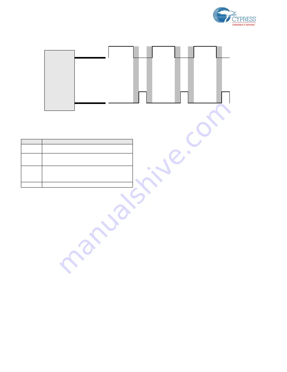
Figure 17-3. Dead Band Functional Overview
Mode bits are encoded for kill options and are detailed in the
following table.
When the block is initially enabled, both outputs are low.
After enabling, a positive or negative edge of the incoming
PWM reference enables the counter. The counter counts
down from the period value to terminal count. At terminal
count, the counter is disabled and the selected phase is
asserted high. On the opposite edge of the PWM input, the
output that was high is negated low and the process is
repeated with the opposite phase. This results in the gener-
ation of a two phase non-overlapping clock matching the fre-
quency and pulse width of the incoming PWM reference, but
separated by a dead time derived from the period and the
input clock.
There is a deterministic relationship between the incoming
PWM reference and the output phases. The positive edge of
the reference causes the primary output to be asserted to '1'
and the negative edge of the reference causes the auxiliary
output to be asserted to '1'.
17.1.8.1
Usability Exceptions
The following are usability exceptions for the Dead Band
function.
1. The Dead Band function may not be chained.
2. Programming a dead band period value of 00h is not
supported. The block output is undefined under this con-
dition.
3. If the period (of either the
or the
the reference input) is less than the programmed dead
time, than the associated output phase will be held low.
4. DR0 may only be read (to transfer DR0 data to DR2)
when the block is disabled.
5. If the asynchronous KILL signal is being used in a given
application, the output of the dead band cannot be con-
nected directly to the input of another digital block in the
same row. Because the kill is asynchronous, the digital
block output must be resynchronized through a row input
before using it as a digital block input.
17.1.8.2
Block Interrupt
The Dead Band block has two interrupt sources. The default
one is the Phase 1 primary output clock. When the KILL sig-
nal is asserted, the interrupt follows the same behavior of
the Phase 1 output with respect to the various KILL modes.
When KILL_INT is selected the KILL signal itself becomes
interrupt. This is the second choice.
However, set KILL_INT
only in KILL-Sync and KILL-Async mode
.
17.1.9
PWMDBL Function
The PWMDBL is an integrated dead band PWM. From a
functional perspective, it combines the counter and dead
band function in a single block with limited dead band width
selections. A PWMDBL consists of a period register, a syn-
chronous down counter, a compare register, and a dead
band width register. The PWMDBL counter function is identi-
cal to the Counter function, with the following exceptions:
■
There is no counter gate input. The counting down is
controlled by different sub modes.
■
The multi-shot mode in PWMDBL is called PPG (Pro-
grammable Pulse Generator) mode. The function is not
disabled at last-shot but instead stops counting. Hard-
ware or software start (write one again to ‘EN’ bit)
resumes the counting. Similarly, if a last shot occurs, and
the start bit is high, counting continues, and the high of
START does not affect the running counting.
D
e
a
d
b
a
n
d
D
e
a
d
b
a
n
d
D
e
a
d
b
a
n
d
D
e
a
d
b
a
n
d
D
e
a
d
b
a
n
d
Primary
Output
Auxiliary
Output
Dead
Band
Function
Table 17-6. Dead Band Kill Options
Mode [1:0]
Description
00b
Synchronous Restart KILL mode. Internal state is reset and
reference edges are ignored, until the KILL signal is negated.
01b
Disable KILL mode. Block is disabled. KILL signal must be
negated and user must re-enable the block in firmware to
resume operation.
10b
Asynchronous KILL mode. Outputs are low only for the dura-
tion that the KILL signal is asserted, subject to a minimum
disable time between one-half to one and one-half clock
cycles. Internal state is unaffected.
11b
Reserved
Summary of Contents for CY8C28 series
Page 65: ...64 CY8C28xxx PSoC Programmable System on Chip TRM Document No 001 52594 Rev G RAM Paging ...
Page 125: ...124 CY8C28xxx PSoC Programmable System on Chip TRM Document No 001 52594 Rev G ...
Page 311: ...310 CY8C28xxx PSoC Programmable System on Chip TRM Document No 001 52594 Rev G IDAC_CR0 1 FDh ...
Page 317: ...316 CY8C28xxx PSoC Programmable System on Chip TRM Document No 001 52594 Rev G ...
Page 393: ...392 CY8C28xxx PSoC Programmable System on Chip TRM Document No 001 52594 Rev G ...
Page 477: ...476 CY8C28xxx PSoC Programmable System on Chip TRM Document No 001 52594 Rev G Digital Clocks ...
Page 561: ...560 CY8C28xxx PSoC Programmable System on Chip TRM Document No 001 52594 Rev G ...


