X90 mobile modules
140
X90 mobile system User's manual V 1.20 - Translation of the original manual
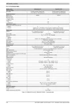
5.3.1.3 Technical data
Model number
X90AO410.04-00
X90AO410.08-00
Short description
I/O module
4 analog outputs or 4 digital inputs
9 to 32 VDC for 1-wire connections
8 analog outputs or 8 digital inputs
9 to 32 VDC for 1-wire connections
General information
B&R ID code
0xEBC4
0xEBC3
Status indicators
-
Electrical isolation
Digital - Analog
No
Certifications
CE
Yes
UN ECE-R10
Yes
Multi-function outputs
Multifunction analog outputs (MF-AO)
Quantity
4
8
Functions
Analog output, 12-bit digital converter resolution, integrated output protection,
digital input, sink/source circuit - configurable per channel, software input filter
Digital inputs
Quantity
0 to 4, depends on the use of
multifunction inputs/outputs
0 to 8, depends on the use of
multifunction inputs/outputs
Input voltage
9 to 32 VDC
Input current at 24 VDC
Typ. 1.3 / 2.6 / 3.7 mA, configurable
Input filter
Hardware
300 µs
Software
Default 1 ms, configurable between 0 and 25 ms in 0.1 ms intervals
Input circuit
Sink/Source, configurable
Input resistance
Typ. 6.5 / 9 / 18 kΩ, configurable
Input delay
<0.5 ms (at 160 µs sampling rate)
Switching threshold
50% supply voltage
Analog outputs
Quantity
0 to 4, depends on the use of
multifunction inputs/outputs
0 to 8, depends on the use of
multifunction inputs/outputs
Output
0 V (high resistance) / 0.1 to 10 V / 0 mA (high resistance) / 0.2 to 20 mA
Max. output current
10 mA (at voltage output)
Digital converter resolution
12-bit
Conversion time
300 µs for all outputs
Settling time for output changes over entire range
700 µs
Switch on/off behavior
Output disabled by semiconductor for startup
Max. error at 25°C
<1%
1)
Output protection
Short circuit protection
Output format
Data type
INT
Voltage
INT 0x0000 - 0x7FFF / 1 LSB = 0x0008 = 2.5 mV
Current
INT 0x0000 - 0x7FFF / 1 LSB = 0x0008 = 4.9 μA
Load per channel
Voltage
Max. 10 mA, load ≥1 kΩ
Current
Max. load is 500 Ω
Short-circuit proof
Current limiting 90 mA
Output filter
1st-order low pass / cutoff frequency 10 kHz
Max. gain drift
Voltage
0.02%/°C
2)
Current
0.04%/°C
2)
Max. offset drift
Voltage
0.01%/°C
1)
Current
0.01%/°C
1)
Max. offset
Voltage
0.1 V
Current
0.2 mA
Error caused by load change
Voltage
Max. 0.11%, from 1 kΩ to 10 MΩ, resistive
Current
Max. 1.4%, from 1 to 500 Ω, resistive
Nonlinearity
<0.02%
1)
Operating conditions
Mounting orientation
Any
Yes
Degree of protection per EN 60529
Up to IP69K
3)
Table 18: X90AO410.04-00, X90AO410.08-00 - Technical data


