


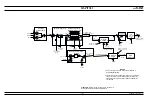
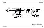


The modulator control signal is received from the A9
PIN Control PCB where it is developed from the
ALC control signal. The modulator control signal
adjusts the gain of the modulator to control the
power level of the RF output signals. In the
691XXB, the modulator is also used for AM and
square wave modulation of the RF output signals.
Amplitude modulation is accomplished by varying
the modulator control signal with the modulating
signal. Square wave modulation is achieved by
switching the modulator on and off at a rate deter-
mined by the modulating square wave.
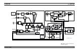
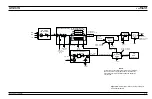
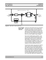
RF Signal
Filtering
The RF signal from the modulator is routed via PIN
switches to the switched low-pass filters. PIN switch
drive current is received from the A9 PIN Control
PCB. A coupler in the switched filter path provides
the RF signal for the down converter. Whenever an
instrument is generating RF signals of <2 GHz
(
£
2.2 GHz for units with Option 21A), a RF signal is
coupled out, through a 8.5 GHz low-pass filter and
connector J3 to the down converter. Another coupler
in the switched filter path of high power switched
filter assemblies provides the RF signal for the
source quadrupler module (refer to Figure 2-7).
Whenever an instrument is generating RF signals of
>40 GHz, a RF signal is coupled out via J4 to the
source quadrupler module.
The switched low-pass filters provide rejection of the
harmonics that are generated by the YIG-tuned os-
cillator. In model 69017B/69117B, the 2 to 8.4 GHz
RF signal from the moulator has three filtering
paths—3.3 GHz, 5.5 GHz, and 8.4 GHz. In all other
690XXC/691XXC models, the 2 to 20 GHz RF signal
from the modulator has four filtering paths and a
through path. The four filtering paths are 3.3 GHz,
5.5 GHz, 8.4 GHz, and 13.5 GHz. Signals above 13.5
GHz are routed via the through path.
After routing through the appropriate path, the 2 to
8.4 GHz or 2 to 20 GHz (2.2 GHz to 20 GHz for units
with Option 21) RF signal is multiplexed by the PIN
switches and goes via a 20 GHz low-pass filter to the
switched filter assembly output connector J2. The
0.01 to 2 GHz (0.01 to 2.2 GHz for units with Option
21A) RF signal, from the down converter, is received
at connector J1, then multiplexed through the same
path to the switched filter output J2.
690XXB/691XXB MM
2-25
FUNCTIONAL
RF DECK
DESCRIPTION
ASSEMBLIES
Summary of Contents for 680 C Series
Page 4: ......
Page 5: ......
Page 13: ...Figure 1 1 Typical Series 690XXB 691XXB Synthesized CW Signal Generator Model 69187B Shown ...
Page 61: ......
Page 97: ......
Page 205: ......
Page 207: ......
Page 221: ......
Page 225: ......
Page 241: ......
Page 259: ......
Page 275: ......
Page 285: ......
Page 289: ......
Page 299: ......
Page 303: ......
Page 315: ......


