


Preliminary Technical Data
UG-1828
Rev. PrC | Page 85 of 338
PIN: CH_ENABLE
CH Analog
t
chEnaSetup
t
chEnaRise2AnaOn
t
chEnaFall2Off
≈
≈
≈
CH_ENABLE Status output on DGPIO
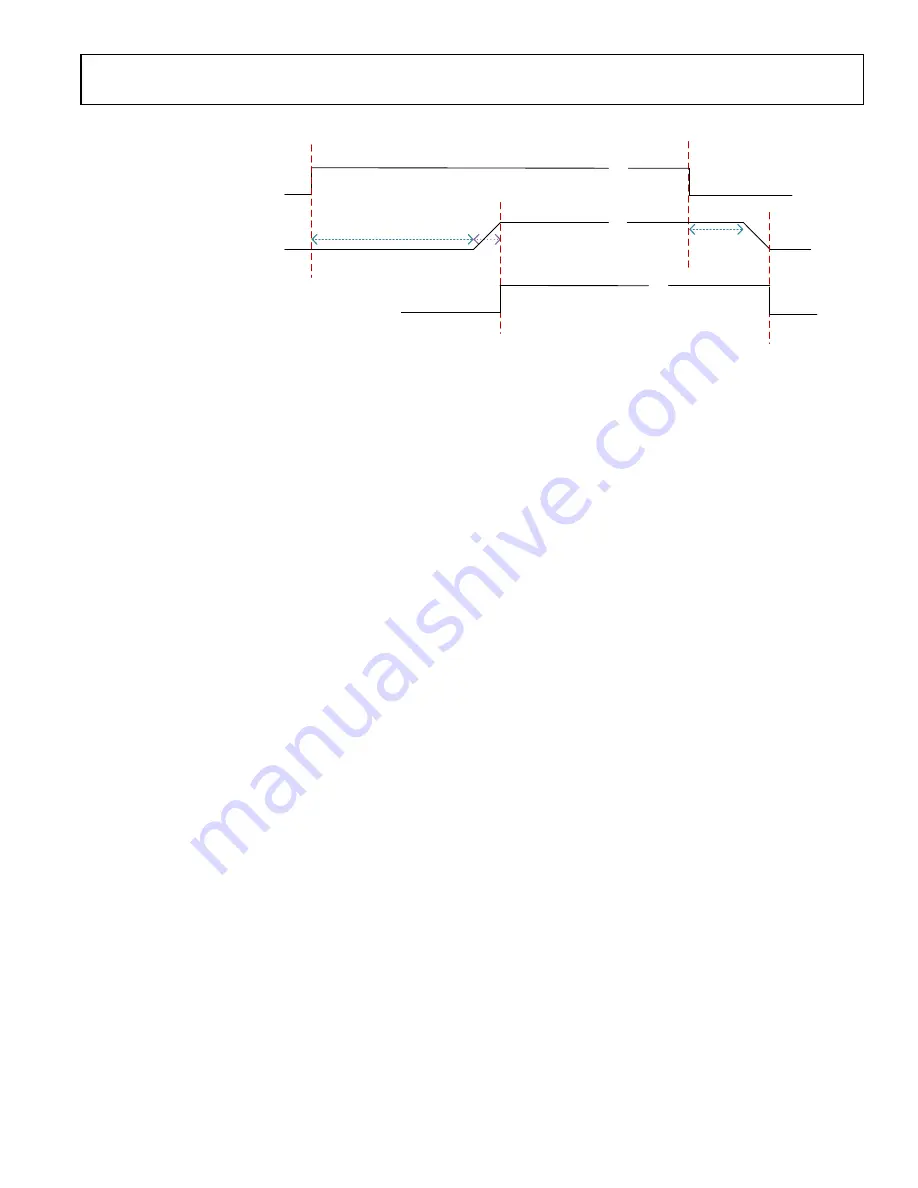
Figure 78 Channel Enable control status output on DGPIO
Figure 78 shows the channel enable signal and its corresponding active output timing on DGPIO, the DGPIO high indicates the start of
the channel analog front end fully up to the end of channel analog front end fully off. If the EnaRise2AnaOn is set to 0, the time from
CH_ENABLE rising edge to DGPIO rising edge is the “enableSetupDelay”. Similarly, if set EnaFall2Off to 0, the time from CH_ENABLE
falling edge to DGPIO falling edge will be the time taken for ADRV9001 to fully power down the analog front end.
This stream status to GPIO debug function can be enabled by API adi_adrv9001_Stream_C0_Gpio_Debug_Set() in chip “Standby” or
“Calibrated” state, the RX1_ENABLE output status will be mapped to DPGIO_0, TX1_ENABLE output status to DGPIO_1,
RX2_ENABLE output status to DGPIO_2 and TX2_ENABLE output status to DGPIO_3, there is no users’ option to configure these
DGPIOs mapping, and once the debug function is enabled, the DGPIO_0~DPGIO_3 will not be available for other functions, no matter
how many channels are configured in the profile. We recommend users using this debug function to do the Tx/Rx ENABLE timing
measurement for a given profile, and disable this function to release the DGPIOs usage once users are done with the measurement.


