


8–26
Chapter 8: Configuration and Remote System Upgrades in Cyclone IV Devices
Configuration
May 2013
Altera Corporation
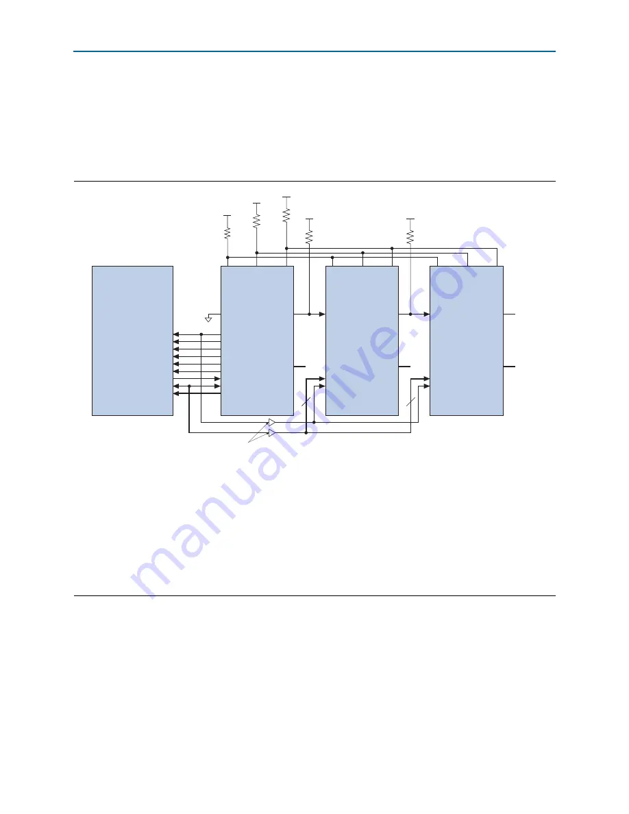
Byte-Wide Multi-Device AP Configuration
The simpler method for multi-device AP configuration is the byte-wide multi-device
AP configuration. In the byte-wide multi-device AP configuration, the LSB of the
DATA[7..0]
pin from the flash and master device (set to the AP configuration scheme)
is connected to the slave devices set to the FPP configuration scheme, as shown in
.
Word-Wide Multi-Device AP Configuration
The more efficient setup is one in which some of the slave devices are connected to the
LSB of the
DATA[7..0]
and the remaining slave devices are connected to the MSB of
the
DATA[15..8]
. In the word-wide multi-device AP configuration, the
nCEO
pin of the
master device enables two separate daisy chains of slave devices, allowing both
chains to be programmed concurrently, as shown in
.
Figure 8–8. Byte-Wide Multi-Device AP Configuration
Notes to
(1) Connect the pull-up resistors to the V
CCIO
supply of the bank in which the pin resides.
(2) Connect the pull-up resistor to the V
CCIO
supply voltage of the I/O bank in which the
nCE
pin resides.
(3) The
nCEO
pin is left unconnected or used as a user I/O pin when it does not feed the
nCE
pin of another device.
(4) The
MSEL
pin settings vary for different configuration voltage standards and POR time. You must set the master device in AP mode and the slave
devices in FPP mode. To connect
MSEL[3..0]
for the master device in AP mode and the slave devices in FPP mode, refer to
. Connect the
MSEL
pins directly to V
CCA
or GND.
(5) The AP configuration ignores the
WAIT
signal during configuration mode. However, if you are accessing flash during user mode with user logic,
you can optionally use the normal I/O to monitor the
WAIT
signal from the Micron P30 or P33 flash.
(6) Connect the repeater buffers between the Cyclone IV E master device and slave devices for
DATA[15..0]
and
DCLK
. All I/O inputs must maintain
a maximum AC voltage of 4.1 V. The output resistance of the repeater buffers must fit the maximum overshoot equation outlined in
and JTAG Pin I/O Requirements” on page 8–5
.
CLK
RST#
CE#
OE#
ADV#
W
E#
W
AIT
DQ[15:0]
A[24:1]
DCLK
nRESET
FLASH_nCE
nOE
nAVD
n
W
E
I/O
(5)
DATA[15..0]
PADD[23..0]
nCE
VCCIO (1)
VCCIO (1)
nCONFIG
nST
A
TUS
CONF_DONE
MSEL[3..0]
(4)
nCEO
N.C.
(3)
Cyclone IV E
Master Device
Micron P30/P33 Flash
GND
DATA[7..0]
DCLK
nCE
nCONFIG
nST
A
TUS
CONF_DONE
MSEL[3..0]
(4)
nCEO
Cyclone IV E Slave Device
DATA[7..0]
DCLK
nCE
nCONFIG
nST
A
TUS
CONF_DONE
MSEL[3..0]
(4)
nCEO
Cyclone IV E Slave Device
VCCIO (2)
VCCIO (2)
Buffers (6)
DQ[7..0]
DQ[7..0]
10 k
Ω
10 k
Ω
10 k
Ω
10 k
Ω
VCCIO (1)
10 k
Ω
Summary of Contents for Cyclone IV
Page 10: ...x Chapter Revision Dates Cyclone IV Device Handbook March 2016 Altera Corporation Volume 1...
Page 14: ...I 2 Section I Device Core Cyclone IV Device Handbook March 2016 Altera Corporation Volume 1...
Page 274: ...vi Contents Cyclone IV Device Handbook February 2015 Altera Corporation Volume 2...
Page 440: ...iv Contents Cyclone IV Device Handbook December 2016 Altera Corporation Volume 3...
Page 442: ...vi Chapter Revision Dates Cyclone IV Device Handbook December 2016 Altera Corporation Volume 3...
Page 446: ......


