TOBY-L4 series - System Integration Manual
UBX-16024839 - R04
System description
Page 17 of 143
Function
Pin Name
Pin No
I/O
Description
Remarks
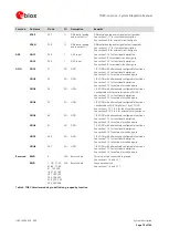
ETH_RX_CLK
43
I
Ethernet Receive
Clock
RGMII: Receive reference clock (RXC).
RMII: Not used.
See section 1.9.6 for functional description.
See section 2.6.6 for external circuit design-in.
ETH_RX_CTL
42
I
Ethernet Receive
Control
RGMII: Control signal for receive data (RXDV on RXC rising
edge; RXDV xor RXER on RXC falling edge).
RMII: Control signal for receive data, contains carrier sense
(CRS) and data valid (RX_DV) information.
See section 1.9.6 for functional description.
See section 2.6.6 for external circuit design-in.
ETH_RXD0
38
I
Ethernet Receive
Data [0]
RGMII: Rx data bit 0 / 4 on RXC rising / falling edges.
RMII: Rx data bit 0 in sync with REF_CLK.
See section 1.9.6 for functional description.
See section 2.6.6 for external circuit design-in.
ETH_RXD1
39
I
Ethernet Receive
Data [1]
RGMII: Rx data bit 1 / 5 on RXC rising / falling edges.
RMII: Rx data bit 1 in sync with REF_CLK.
See section 1.9.6 for functional description.
See section 2.6.6 for external circuit design-in.
ETH_RXD2
40
I
Ethernet Receive
Data [2]
RGMII: Rx data bit 2 / 6 on RXC rising / falling edges.
RMII: Not used.
See section 1.9.6 for functional description.
See section 2.6.6 for external circuit design-in.
ETH_RXD3
41
I
Ethernet Receive
Data [3]
RGMII: Rx data bit 3 / 7 on RXC rising / falling edges.
RMII: Not used.
See section 1.9.6 for functional description.
See section 2.6.6 for external circuit design-in.
ETH_INTR
220
I
Ethernet Interrupt
Input
Input for the detection of an interrupt event in the PHY.
See section 1.9.6 for functional description.
See section 2.6.6 for external circuit design-in.
ETH_MDIO
222
I/O
Ethernet
Management Data
Input Output
Ethernet management data input / output.
See section 1.9.6 for functional description.
See section 2.6.6 for external circuit design-in.
ETH_MDC
223
O
Ethernet
Management Data
Clock
Ethernet management data clock output.
See section 1.9.6 for functional description.
See section 2.6.6 for external circuit design-in.
eMMC
V_MMC
210
O
Multi-Media Card
Interface supply
output
Embedded Multi-Media / SD Card memory supply.
See section 1.10 for functional description.
See section 2.7 for external circuit design-in.
MMC_D0
214
I/O
Multi-Media Card
Data [0]
Embedded Multi-Media / SD Card memory data [0].
See section 1.10 for functional description.
See section 2.7 for external circuit design-in.
MMC_D1
212
I/O
Multi-Media Card
Data [1]
Embedded Multi-Media / SD Card memory data [1].
See section 1.10 for functional description.
See section 2.7 for external circuit design-in.
MMC_D2
217
I/O
Multi-Media Card
Data [2]
Embedded Multi-Media / SD Card memory data [2].
See section 1.10 for functional description.
See section 2.7 for external circuit design-in.
MMC_D3
213
I/O
Multi-Media Card
Data [3]
Embedded Multi-Media / SD Card memory data [3].
See section 1.10 for functional description.
See section 2.7 for external circuit design-in.
MMC_CMD
215
I/O
Multi-Media Card
Command
Embedded Multi-Media / SD Card memory command.
See section 1.10 for functional description.
See section 2.7 for external circuit design-in.
MMC_CLK
216
O
Multi-Media Card
Clock
Embedded Multi-Media / SD Card memory clock.
See section 1.10 for functional description.
See section 2.7 for external circuit design-in.

