TOBY-L4 series - System Integration Manual
UBX-16024839 - R04
Design-in
Page 95 of 143
Connection with u-blox 1.8 V GNSS receivers
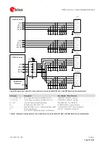
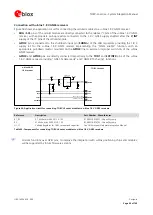
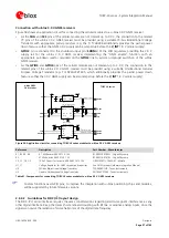
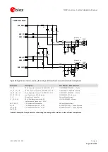
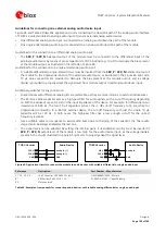
Figure 54 shows an application circuit for connecting the cellular modules to a u-blox 1.8 V GNSS receiver.
SDA
/
SCL
pins of the cellular module are directly connected to the relative I
2
C pins of the u-blox 1.8 V GNSS
receiver, with appropriate pull-up resistors connected to the 1.8 V GNSS supply enabled after the
V_INT
supply of the I
2
C pins of the cellular module.
GPIO2
pin is connected to the shutdown input pin (
SHDNn
) of the LDO regulators providing the 1.8 V
supply rail for the u-blox 1.8 V GNSS receiver implementing the “GNSS enable” function, with an
appropriate pull-down resistor mounted on the
GPIO2
line to avoid an improper switch-on of the u-blox
GNSS receiver.
GPIO3
and
GPIO4
pins are directly connected respectively to the
TXD1
and
EXTINT0
pins of the u-blox
1.8 V GNSS receiver providing “GNSS Tx data ready” and “GNSS RTC sharing” functions.
R1
IN
OUT
GND
GNSS LDO
Regulator
SHDNn
u-blox GNSS
1.8 V receiver
SDA2
SCL2
R2
1V8
1V8
VMAIN
1V8
U1
22
GPIO2
SDA
SCL
C1
TxD1
GPIO3
55
54
24
VCC
R3
GNSS Tx data ready
GNSS supply enabled
TOBY-L4 series
EXTINT0
GPIO4
25
GNSS RTC sharing
Figure 54: Application circuit for connecting TOBY-L4 series modules to u-blox 1.8 V GNSS receivers
Reference
Description
Part Number - Manufacturer
R1, R2
4.7 k
Resistor 0402 5% 0.1 W
RC0402JR-074K7L - Yageo Phycomp
R3
47 k
Resistor 0402 5% 0.1 W
RC0402JR-0747KL - Yageo Phycomp
U1, C1
Voltage Regulator for GNSS receiver and capacitor
See GNSS receiver Hardware Integration Manual
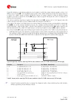
Table 39: Components for connecting TOBY-L4 series modules to u-blox 1.8 V GNSS receivers
Custom functions over GPIO pins, to improve the integration with u-blox positioning chips and modules,
will be supported by future firmware versions.

