TOBY-L4 series - System Integration Manual
UBX-16024839 - R04
Appendix
Page 138 of 143
TOBY-L2
TOBY-L4
Pin No
Pin Name
Description
Pin Name
Description
Remarks for migration
47-49
RSVD
Reserved
RSVD
Reserved
50
I2S_WA
I
2
S Word Alignment
I2S_WA
I
2
S Word Alignment
I2S / GPIO
I2S
51
I2S_TXD
I
2
S Data Output
I2S_TXD
I
2
S Data Output
I2S / GPIO
I2S
52
I2S_CLK
I
2
S Clock
I2S_CLK
I
2
S Clock
I2S / GPIO
I2S
53
I2S_RXD
I
2
S Data Input
I2S_RXD
I
2
S Data Input
I2S / GPIO
I2S
54
SCL
I
2
C Clock Output
25
SCL
I
2
C Clock Output
26
55
SDA
I
2
C Data I/O
SDA
I
2
C Data I/O
56
SIM_CLK
SIM Clock Output
SIM_CLK
SIM Clock Output
57
SIM_IO
SIM Data I/O
SIM_IO
SIM Data I/O
58
SIM_RST
SIM Reset Output
SIM_RST
SIM Reset Output
59
VSIM
SIM Supply Output
VSIM
SIM Supply Output
60
GPIO5
GPIO
GPIO5
GPIO
61
GPIO6
GPIO
GPIO6
GPIO
62
HOST_SELECT1 Not supported
HOST_SELECT1 GPIO
Not supported
GPIO / EINT
63
SDIO_D2
SDIO serial data [2]
SDIO_D2
SDIO serial data [2]
64
SDIO_CLK
SDIO serial clock
SDIO_CLK
SDIO serial clock
65
SDIO_CMD
SDIO command
SDIO_CMD
SDIO command
66
SDIO_D0
SDIO serial data [0]
SDIO_D0
SDIO serial data [0]
67
SDIO_D3
SDIO serial data [3]
SDIO_D3
SDIO serial data [3]
68
SDIO_D1
SDIO serial data [1]
SDIO_D1
SDIO serial data [1]
69
GND
Ground
GND
Ground
70-72
VCC
Module Supply Input
3.40 V – 4.35 V normal range
3.20 V – 4.35 V extended range
VCC
Module Supply Input
3.40 V – 4.40 V normal range
3.00 V – 4.50 V extended range
Larger operating ranges on TOBY-L4
73-74
GND
Ground
GND
Ground
75
ANT_DET
Antenna Detection Input
ANT_DET
Antenna Detection Input
76
GND
Ground
GND
Ground
77
RSVD
Reserved
RSVD
Reserved
78-80
GND
Ground
GND
Ground
81
ANT1
RF Antenna Input/Output
Up to six LTE bands
Up to five 3G bands
Up to four 2G bands
ANT1
RF Antenna Input/Output
Up to seven LTE bands
Up to three 3G bands
Up to four 2G bands
No RF functional difference
Different operating bands (Figure 73)
82-83
GND
Ground
GND
Ground
84
RSVD
Reserved
RSVD
Reserved
85-86
GND
Ground
GND
Ground
87
ANT2
RF Antenna Input
ANT2
RF Antenna Input
No RF functional difference
Different operating bands (Figure 73)
88-90
GND
Ground
GND
Ground
91
RSVD
Reserved
RSVD
Reserved
92-152
GND
Ground
GND
Ground
152-248
Pins not available
Additional functions
Not available
Additional functions
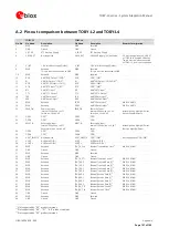
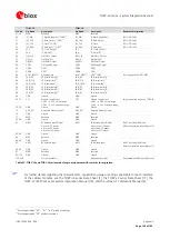
Table 52: TOBY-L2 and TOBY-L4 series modules pin assignment with remarks for migration
For further details regarding the characteristics, capabilities, usage or settings applicable for each interface
of the cellular modules, see the
TOBY-L4 series
[1], the
TOBY-L2 series Data Sheet
[17], the
TOBY-L2 / MPCI-L2 series System Integration Manual
[18], and the
u-blox AT Commands Manual
25
Not supported by "00", "01", "60" product versions
26
Not supported by "50" product versions

