TOBY-L4 series - System Integration Manual
UBX-16024839 - R04
Design-in
Page 78 of 143
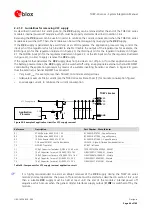
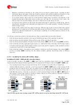
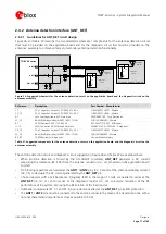
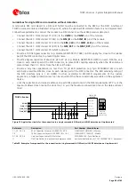
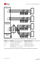
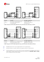
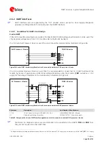
The DC impedance at the RF port for some antennas may be a DC open (e.g. linear monopole) or a DC short to
reference GND (e.g. PIFA antenna). For those antennas without the diagnostic circuit of Figure 36, the measured
DC resistance is always at the limits of the measurement range (respectively open or short), and there is no
means to distinguish between a defect on the antenna path with similar characteristics (respectively: removal of
linear antenna or RF cable shorted to GND for a PIFA antenna).
Furthermore, any other DC signal injected to the RF connection from an ANT connector to a radiating element
will alter the measurement and produce invalid results for antenna detection.
It is recommended to use an antenna with a built-in diagnostic resistor in the range from 5 k
to 30 k
to assure good antenna detection functionality and avoid a reduction of module RF performance. The
choke inductor should exhibit a parallel Self Resonance Frequency (SRF) in the range of 1 GHz to improve
the RF isolation of the load resistor.
For example:
Consider an antenna with a built-in DC load resistor of 15 k
. Using the +UANTR AT command, the module
reports the resistance value evaluated from the antenna connector provided on the application board to GND:
Reported values close to the used diagnostic resistor nominal value (i.e. values from 13 k
to 17 k
if a
15 k
diagnostic resistor is used) indicate that the antenna is properly connected.
Values close to the measurement range maximum limit (approximately 50 k
) or an open-circuit
“over range” report (see the
u-blox AT Commands Manual
[2]) means that that the antenna is not
connected or the RF cable is broken.
Reported values below the measurement range minimum limit (1 k
) indicate a short to GND at the
antenna or along the RF cable.
Measurement inside the valid measurement range and outside the expected range may indicate an incorrect
connection, damaged antenna or wrong value of antenna load resistor for diagnostics.
The reported value could differ from the real resistance value of the diagnostic resistor mounted inside the
antenna assembly due to the antenna cable length, the antenna cable capacity or the measurement method
used.
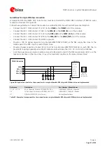
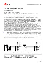
If the primary / secondary antenna detection function is not required by the customer application, the
ANT_DET
pin can be left unconnected and the
ANT1
/
ANT2
pins can be directly connected to the
related antenna connector by means of a 50
transmission line as illustrated in Figure 35.
2.4.2.2
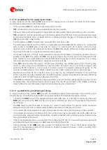
Guidelines for ANT_DET layout design
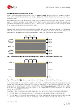
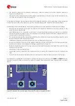
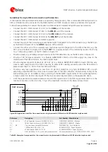
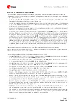
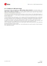
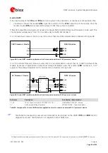
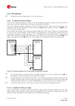
The recommended layout for the primary antenna detection circuit to be provided on the application board to
achieve the primary antenna detection functionality, implementing the recommended schematic illustrated in
Figure 36 and Table 27, is explained here:
The
ANT1
/
ANT2
pins must be connected to the antenna connector by means of a 50
transmission line,
implementing the design guidelines described in section 2.4.1 and the recommendations of the SMA
connector manufacturer.
DC blocking capacitor at
ANT1
/
ANT2
pins (C2, C3) must be placed in series to the 50
RF line.
The
ANT_DET
pin must be connected to the 50
transmission line by means of a sense line.
Choke inductors in series at the
ANT_DET
pin (L1, L2) must be placed so that one pad is on the 50
transmission line and the other pad represents the start of the sense line to the
ANT_DET
pin.
The additional components (R1, C1 and D1) on the
ANT_DET
line must be placed as ESD protection.

