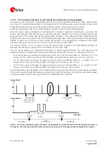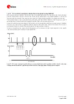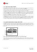
TOBY-L4 series - System Integration Manual
UBX-16024839 - R04
System description
Page 22 of 143
1.5
Supply interfaces
1.5.1
Module supply input (VCC)
The modules must be supplied via the three
VCC
pins that represent the module power supply input.
The
VCC
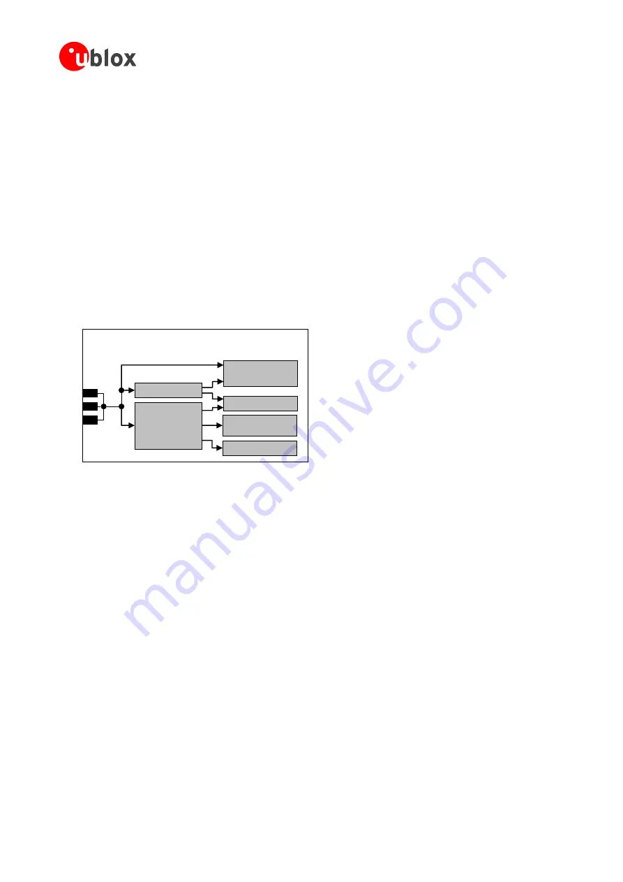
pins are internally connected to the RF power amplifier and to the integrated Power Management Unit:
all supply voltages needed by the module are generated from the
VCC
supply by integrated voltage regulators,
including the Real Time Clock supply,
V_INT
generic digital interfaces supply,
VSIM
SIM card supply,
V_ETH
RGMII interface supply,
V_MMC
eMMC interface supply, and any other internal rail.
During operation, the current drawn by the TOBY-L4 series modules through the
VCC
pins can vary by several
orders of magnitude. This ranges from the pulse of current consumption during GSM transmitting bursts at
maximum power level in connected mode (as described in section 1.5.1.2) to the low current consumption
during low power idle mode with power saving enabled (as described in section 1.5.1.5).
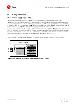
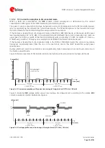
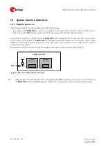
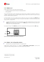
Figure 3 provides a simplified block diagram of the TOBY-L4 series modules’ internal VCC supply routing.
72
VCC
71
VCC
70
VCC
TOBY-L4 series
Power
Management
Unit
Memory
Baseband
Processor
Transceiver
RF PMU
Cellular
Power Amplifiers
Figure 3: TOBY-L4 series modules’ internal VCC supply routing simplified block diagram

