TOBY-L4 series - System Integration Manual
UBX-16024839 - R04
System description
Page 12 of 143
1.3
Pin-out
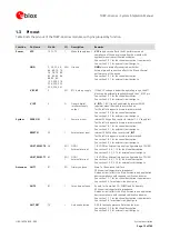
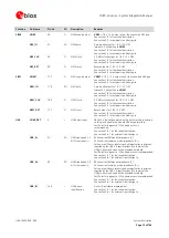
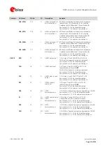
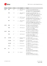
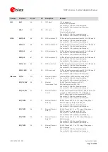
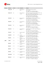
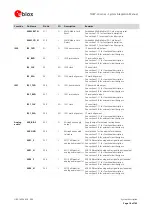
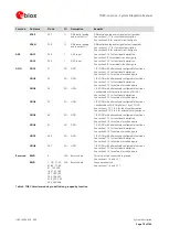
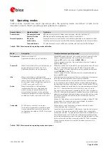
Table 4 lists the pin-out of the TOBY-L4 series modules, with pins grouped by function.
Function
Pin Name
Pin No
I/O
Description
Remarks
Power
VCC
70,71,72
I
Module supply input
VCC
supply circuit affects the RF performance and
compliance of the device integrating the module with
applicable required certification schemes.
See section 1.5.1 for functional description / requirements.
See section 2.2.1 for external circuit design-in.
GND
2, 30, 32, 44,
46, 69, 73, 74,
76, 78, 79, 80,
82, 83, 85, 86,
88-90, 92-
152, 209, 219,
226, 229, 232,
235, 238, 241
N/A
Ground
GND
pins are internally connected each other.
External ground connection affects the RF and thermal
performance of the device.
See section 1.5.1 for functional description.
See section 2.2.1 for external circuit design-in.
V_BCKP
3
I/O
RTC back-up supply
If the VCC voltage is below the operating range, the RTC
block can be externally supplied through the V_BCKP pin.
See section 1.5.2 for functional description.
See section 2.2.2 for external circuit design-in.
V_INT
5
O
Generic digital
interfaces supply
output
V_INT
= 1.8 V (typical) generated by internal DC/DC
regulator when the module is switched on.
Test-Point for diagnostic access is recommended.
See section 1.5.3 for functional description.
See section 2.2.3 for external circuit design-in.
System
PWR_ON
20
I
Power-on input
Internal 35 k
pull-up resistor to internal 1.3 V supply rail.
Test-Point for diagnostic access is recommended.
See section 1.6.1 for functional description.
See section 2.3.1 for external circuit design-in.
RESET_N
23
I
External reset input
Internal 100 k
pull-up resistor to
V_INT
.
Test-Point for diagnostic access is recommended.
See section 1.6.3 for functional description.
See section 2.3.2 for external circuit design-in.
HOST_SELECT0
26
I/O /
I
GPIO /
External Interrupt
1.8 V GPIO or External Interrupt configurable by uCPU API.
See sections 1.6.4, 1.13 for functional description.
See sections 2.3.3, 2.10 for external circuit design-in.
HOST_SELECT1
62
I/O /
I
GPIO /
External Interrupt
1.8 V GPIO or External Interrupt configurable by uCPU API.
See sections 1.6.4, 1.13 for functional description.
See sections 2.3.3, 2.10 for external circuit design-in.
Antennas
ANT1
81
I/O
Primary antenna
Main Tx / Rx antenna interface.
50
nominal characteristic impedance.
Antenna circuit affects the RF performance and application
device compliance with required certification schemes.
See section 1.7.1 for functional description / requirements.
See section 2.4 for external circuit design-in.
ANT2
87
I
Secondary antenna
Rx only for Down-Link CA, MIMO and Rx diversity.
50
nominal characteristic impedance.
Antenna circuit affects the RF performance and application
device compliance with required certification schemes.
See section 1.7.1 for functional description / requirements.
See section 2.4 for external circuit design-in.
ANT_DET
75
I
Antenna detection
ADC for antenna presence detection function.
See section 1.7.2 for functional description.
See section 2.4.2 for external circuit design-in.

