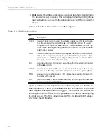
Wait-State Generator
8-14
8.5
Wait-State Generator
Wait states are necessary when you want to interface the ’C2xx with slower
external logic and memory. By adding wait states, you lengthen the time the
CPU waits for external memory or an external I/O port to respond when the
CPU reads from or writes to that memory or port. Specifically, the CPU waits
one extra cycle (one CLKOUT1 cycle) for every wait state. The wait states op-
erate on CLKOUT1 cycle boundaries.
To avoid bus conflicts, writes from the ’C2xx always take at least two
CLKOUT1 cycles.
The ’C2xx offers two options for generating wait states:
-
The READY signal. With the READY signal, you can externally generate
any number of wait states.
-
The on-chip wait-state generator. With this generator, you can generate
zero to seven wait states.
8.5.1
Generating Wait States With the READY Signal
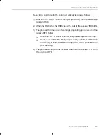
When READY is low, the ’C2xx waits one CLKOUT1 cycle and checks READY
again. The ’C2xx will not continue executing until READY is driven high; there-
fore, if the READY signal is not used, it should be pulled high during external
accesses.
Again, the READY pin can be used to generate any number of wait states.
However, even when the ’C2xx operates at full speed, it may not respond fast
enough to provide a READY-based wait state for the first cycle. For extended
wait states using external READY logic, the on-chip wait-state generator
should be programmed to generate at least one wait state.
The READY pin has no effect on accesses to
internal memory or I/O registers,
except in the case of the ’C209 (see Section 11.2,
’C209 Memory and I/O
Spaces, on page 11-5.) For a ’C2xx device with a boot loader, READY must
be high at boot time.
8.5.2
Generating Wait States With the ’C2xx Wait-State Generator
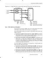
For devices other than the ’C209, the software wait-state generator can be
programmed to generate zero to seven wait states for a given off-chip memory
space (lower program, upper program, data, or I/O), regardless of the state of
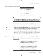
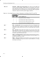
the READY signal. This wait-state generator has the bit fields shown in
Figure 8–6 and described after the figure. For a description of the ’C209 wait-


