Device-Specific Information
4-36
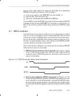
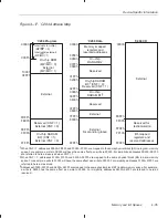
You select or deselect the ROM by changing the level on the MP/MC pin at re-
set:
-
MP/MC = 0 at reset. The device is configured as a microcomputer. The
on-chip ROM is enabled and is accessible at addresses 0000h–0FFFh.
The device fetches the reset vector from on-chip ROM.
-
MP/MC = 1 at reset. The device is configured as a microprocessor, and
addresses 0000h–0FFFh are used to access external memory. The de-
vice fetches the reset vector from external memory.
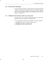
Regardless of the value of MP/MC, the ’C2xx fetches its reset vector at location
0000h of program memory.
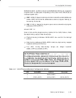
DARAM blocks B1 and B2 are fixed, but DARAM block B0 may be mapped to
program space or data space, depending on the value of the CNF bit (bit 12
of status register ST1):
-
CNF = 0. B0 is mapped to data space and is accessible at data addresses
0200h–02FFh. Note that the addressable external
program memory in-
creases by 512 words.
-
CNF = 1. B0 is mapped to program space and is accessible at program
addresses FF00h–FFFFh.
At reset, CNF = 0.
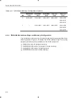
Table 4–7 lists the available program memory configurations for the ’C204;
Table 4–8 lists the data-memory configurations. Note these facts:
-
Program-memory addresses 0000h–003Fh are used for the interrupt
vectors.
-
Data-memory addresses 0000h–005Fh contain on-chip memory-mapped
registers and reserved memory.
-
Two other on-chip data-memory ranges are always reserved:
0080h–01FFh and 0400h–07FFh.
Do Not Write to Reserved Addresses
To avoid unpredictable operation of the processor, do not write to
any addresses labeled Reserved. This includes any data-memory
address in the range 0000h–005Fh that is not designated for an
on-chip register and any I/O address in the range FF00h–FFFFh
that is not designated for an on-chip register.

