’C209 On-Chip Peripherals
11-16
Bit 4
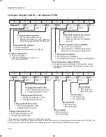
TSS — Timer stop status bit. TSS is a 1-bit flag that stops or starts the timer. To stop
the timer, set TSS to 1. To start or restart the timer, set TSS to 0. At reset, TSS is
cleared to 0 and the timer immediately starts.
Bits 3–0
TDDR —Timer divide-down register. Every (TDDR + 1) CLKOUT1 cycles, the timer
counter register (TIM) decrements by one. At reset, the TDDR bits are cleared to 0.
If you want to increase the overall timer count by an integer factor, write this factor
minus one to the four TDDR bits. When the prescaler counter (PSC) value is 0, one
CLKOUT1 cycle later, the contents of the TDDR reload the PSC, and the TIM decre-
ments by 1. TDDR also reloads the PSC whenever the timer reload bit (TRB) is set
by software.
11.4.3 ’C209 Wait-State Generator
As with other ’C2xx devices, the ’C209 offers two options for generating wait
states:
-
The READY signal. With the READY signal, you can externally generate
any number of wait states.
-
The on-chip wait-state generator. With the ’C209 wait-state generator,
you can internally generate zero or one wait state.
The ’C209 wait-state generator inserts a wait state to a given memory space
(data, program, or I/O) if the corresponding bit in WSGR is set to 1, regardless
of the condition of the READY signal. As with other ’C2xx devices, the READY
signal can then be used to further extend wait states. The WSGR control bits
are all set to 1 by reset, so that the device can operate from slow memory after
reset. To avoid bus conflicts, writes from the ’C209 always take two CLKOUT1
cycles each.
To control the wait-state generator, you read from or write to the wait-state gen-
erator control register (WSGR), mapped to I/O memory location FFFFh.
Figure 11–5 shows the register’s bit layout, and descriptions of the bits follow.
The WSGR also enables or disables address visibility mode.


