background image

Instruction Set Comparison Table

B-13

TMS320C1x/C2x/C2xx/C5x Instruction Set Comparison

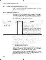
Syntax

Description

5x

2xx

2x

1x

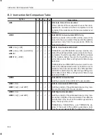
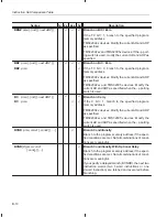
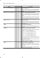
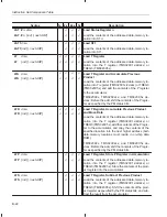
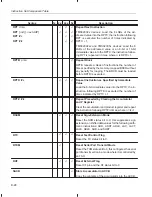
BLKD

dma1, dma2

BLKD

dma1, {ind} [, next ARP]

Block Move From Data Memory to Data Memory

Move a block of words from one location in data mem-
ory to another location in data memory. Modify the cur-
rent AR and ARP as specified. RPT or RPTK must be
used with BLKD, in the indirect addressing mode, if
more than one word is to be moved. The number of
words to be moved is 1 greater than the number
contained in RPTC at the beginning of the instruction.

BLKP

pma, dma

BLKP

pma, {ind} [, next ARP]

Block Move From Program Memory to Data
Memory

Move a block of words from a location in program
memory to a location in data memory. Modify the cur-
rent AR and ARP as specified. RPT or RPTK must be
used with BLKD, in the indirect addressing mode, if
more than one word is to be moved. The number of
words to be moved is 1 greater than the number
contained in RPTC at the beginning of the instruction.

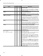
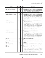
BLPD #

pma, dma

BLPD #

pma, {ind} [, next ARP]

BLPD BMAR, 

dma

BLPD BMAR, {

ind} [, next ARP]

Block Move From Program Memory to Data 
Memory

Copy a block of program memory into data memory.
The block of program memory is pointed to by 

src, and

the destination block of data memory is pointed to by
dst.

TMS320C2xx devices: The word of the source space
can be pointed to with a long immediate value. You can
use the RPT instruction with BLPD to move consecu-
tive words that are pointed at indirectly in data memory
to a contiguous program-memory space.

TMS320C5x devices: The word of the source space
can be pointed to with a long immediate value or the
contents of the BMAR. You can use the RPT instruc-
tion with BLPD to move consecutive words that are
pointed at indirectly in data memory to a contiguous
program-memory space.

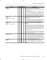
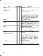
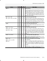
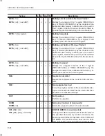
BLZ

pma

BLZ

pma [, {ind} [, next ARP] ]

Branch if Accumulator < Zero

If the contents of the accumulator are < 0, branch to the
specified program-memory address.

TMS320C2x devices: Modify the current AR and ARP
as specified.

TMS320C2xx and TMS320C5x devices: Modify the
current AR and ARP as specified when the –p porting
switch is used.

Содержание TMS320C2XX

Страница 1: ...TMS320C2xx User s Guide Literature Number SPRU127B Manufacturing Part Number D412008 9761 revision A January 1997 Printed on Recycled Paper...

Страница 2: ...ED INTENDED AUTHORIZED OR WARRANTED TO BE SUITABLE FOR USE IN LIFE SUPPORT APPLICATIONS DEVICES OR SYSTEMS OR OTHER CRITICAL APPLICATIONS Inclusion of TI products in such applications is understood to...

Страница 3: ...eviated for example TMS320C203 will be abbreviated as C203 How to Use This Manual Chapter 1 Introduction summarizes the TMS320 family of products and then introduces the key features of the TMS320C2xx...

Страница 4: ...n Chapter 2 Architectural Overview Input output ports Chapter 4 Memory and I O Spaces Interrupts Chapter 5 Program Control Memory configuration Chapter 4 Memory and I O Spaces Memory interfacing Chapt...

Страница 5: ...dentify an optional parameter If you use an optional parameter you specify the information within the brackets you do not type the brackets themselves You separate each optional operand from required...

Страница 6: ...1x TMS320C2x TMS320C2xx and TMS320C5x assembly language tools and the C compiler for the C1x C2x C2xx and C5x devices The installation for MS DOS OS 2 SunOS and Solaris systems is covered TMS320C1x C2...

Страница 7: ...11 describes the TMS320 family of digital signal processors and the tools that support these devices Included are code generation tools compilers assemblers linkers etc and system integration and debu...

Страница 8: ...1995 Developing Nations Take Shine to Wireless Russell MacDonald Kara Schmidt and Kim Higden EE Times October 2 1995 Digital Signal Processing Solutions Target Vertical Application Markets Ron Wages E...

Страница 9: ...n Chip Multiprocessing Melds DSPs Karl Guttag and Doug Deao DSP Series Part III EE Times July 18 1994 Real Time Control Gregg Bennett Appliance Manufacturer May 1995 Speech Recognition P K Rajasekaran...

Страница 10: ...ademark of Hewlett Packard Company Intel is a trademark of Intel Corporation MS DOS and Windows are registered trademarks of Microsoft Corporation PAL is a registered trademark of Advanced Micro Devic...

Страница 11: ...an Factory Repair 33 4 93 22 25 40 Europe Customer Training Helpline Fax 49 81 61 80 40 10 Asia Pacific Literature Response Center 852 2 956 7288 Fax 852 2 956 2200 Hong Kong DSP Hotline 852 2 956 726...

Страница 12: ...s and scanning logic 2 1 C2xx Bus Structure 2 3 2 2 Central Processing Unit 2 5 2 2 1 Central Arithmetic Logic Unit CALU and Accumulator 2 5 2 2 2 Scaling Shifters 2 5 2 2 3 Multiplier 2 6 2 2 4 Auxil...

Страница 13: ...ss maps and descriptions of the HOLD direct memory access operation and the on chip boot loader 4 1 Overview of the Memory and I O Spaces 4 2 4 1 1 Pins for Interfacing to External Memory and I O Spac...

Страница 14: ...al Calls 5 12 5 4 5 Conditional Returns 5 12 5 5 Repeating a Single Instruction 5 14 5 6 Interrupts 5 15 5 6 1 Interrupt Operation Three Phases 5 15 5 6 2 Interrupt Table 5 16 5 6 3 Maskable Interrupt...

Страница 15: ...Examples 7 18 7 3 Instruction Descriptions 7 20 8 On Chip Peripherals 8 1 Introduces the TMS320C2xx on chip peripherals Describes the clock generator the CLKOUT1 pin control register the timer the wai...

Страница 16: ...FIFO Buffers 9 15 9 5 Transmitter Operation 9 16 9 5 1 Burst Mode Transmission With Internal Frame Sync FSM 1 TXM 1 9 16 9 5 2 Burst Mode Transmission With External Frame Sync FSM 1 TXM 0 9 18 9 5 3...

Страница 17: ...4 C209 On Chip Peripherals 11 14 11 4 1 C209 Clock Generator Options 11 14 11 4 2 C209 Timer Control Register TCR 11 15 11 4 3 C209 Wait State Generator 11 16 A Register Summary A 1 Is a concise centr...

Страница 18: ...tocol E 4 E 3 Emulator Cable Pod E 5 E 4 Emulator Cable Pod Signal Timing E 6 E 5 Emulation Timing Calculations E 7 E 6 Connections Between the Emulator and the Target System E 10 E 6 1 Buffering Sign...

Страница 19: ...nal Program Memory 4 6 4 2 Pages of Data Memory 4 7 4 3 Interface With External Local Data Memory 4 10 4 4 GREG Register Set to Configure 8K for Global Data Memory 4 12 4 5 Global and Local Data Memor...

Страница 20: ...ster I O Space Address FFE8h 8 7 8 4 Timer Functional Block Diagram 8 8 8 5 C2xx Timer Control Register TCR I O Space Address FFF8h 8 11 8 6 C2xx Wait State Generator Control Register WSGR I O Space A...

Страница 21: ...Pod Timings E 6 E 4 Emulator Connections Without Signal Buffering E 10 E 5 Emulator Connections With Signal Buffering E 11 E 6 Target System Generated Test Clock E 12 E 7 Multiprocessor Connections E...

Страница 22: ...ress Loading to the Program Counter 5 4 5 3 Conditions for Conditional Calls and Returns 5 10 5 4 Groupings of Conditions 5 11 5 5 C2xx Interrupt Locations and Priorities 5 16 5 6 Reset Values of On C...

Страница 23: ...ts IO0 IO3 and DIO0 DIO3 10 16 11 1 C209 Program Memory Configuration Options 11 8 11 2 C209 Data Memory Configuration Options 11 9 11 3 C209 On Chip Registers Mapped to I O Space 11 9 11 4 C209 Inter...

Страница 24: ...Delay Loops delay asm C 8 C 5 Testing and Using the Timer timer asm C 9 C 6 Testing and Using Interrupt INT1 intr1 asm C 10 C 7 Implementing a HOLD Operation hold asm C 11 C 8 Testing and Using Interr...

Страница 25: ...Do Not Write to Test Emulation Addresses 4 8 Obtain the Proper Timing Information 4 9 Do Not Write to Reserved Addresses 4 24 Do Not Write to Reserved Addresses 4 33 Do Not Write to Reserved Addresses...

Страница 26: ...2xx is source code compatible with the TMS320C2x Much of the code written for the C2x can be reassembled to run on a C2xx device In addition the C2xx generation is upward compatible with the C5x gener...

Страница 27: ...he TMS32010 the first fixed point DSP in the TMS320 family Before the end of the year Electronic Products magazine awarded the TMS32010 the title Product of the Year Today the TMS320 family consists o...

Страница 28: ...TMS320 Family 1 3 Introduction Figure 1 1 TMS320 Family Performance...

Страница 29: ...neration Windowing 3 D rotation Animation digital maps Homomorphic processing Image compression transmission Image enhancement Pattern recognition Robot vision Workstations Numeric control Power line...

Страница 30: ...design for increased performance and versatility Modular architectural design for fast development of additional spin off devices Advanced IC processing technology for increased performance Fast and...

Страница 31: ...space 64K words of I O space and 32K words of global space J 544 words of dual access on chip RAM 288 words for data and 256 words for program data J 4K words on chip ROM or 32K words on chip flash m...

Страница 32: ...it state generator for program data and I O memory spaces J Oscillator and phase locked loop PLL to implement clock options 1 2 4 and 2 only 2 and 2 available on C209 J CLK register for turning the CL...

Страница 33: ...2 1 shows an overall block diagram of the C2xx Note All C2xx devices use the same central processing unit CPU bus structure and instruction set but the C209 has some notable differences For exam ple...

Страница 34: ...sh SARAM DARAM B0 DARAM B1 B2 ST0 IMR IFR GREG ST1 MUX Input shifter Multiplier 16 16 TREG MUX PREG Product shifter Accumulator Output shifter Auxiliary registers 8 16 CALU ARAU MUX MUX MUX MUX AR0 DR...

Страница 35: ...auxiliary register arithmetic unit ARAU DWEB The data write bus carries data to both program memory and data memory Having separate address buses for data reads DRAB and data writes DWAB allows the C...

Страница 36: ...Memory control MULTI_DSP CLOCK PLL Interrupts JTAG TEST Central processing unit CPU Auxiliary registers registers Status ARAU CALU Accumulator Multiplier Product shifter Input shifter PREG TREG Outpu...

Страница 37: ...h order word bits 31 through 16 and a low order word bits 15 through 0 Assembly language instructions are provided for storing the high and low order accumulator words to data memory 2 2 2 Scaling Shi...

Страница 38: ...ion correlation and filtering The ef fective execution time of each multiplication instruction can be as short as one CPU cycle 2 2 4 Auxiliary Register Arithmetic Unit ARAU and Auxiliary Registers Th...

Страница 39: ...88 288 288 Data program words 256 256 256 256 SARAM words 4K 4K The C2xx also has CPU registers that are mapped in data memory space and peripheral registers that are mapped in on chip I O space The C...

Страница 40: ...f chip data and program memory Code can be booted from off chip ROM and then executed at full speed once it is loaded into the on chip SARAM Because the SARAM can be mapped to program and or data memo...

Страница 41: ...nically erasable and programmable and non volatile Each block of flash memory will have a set of control registers that allow for erasing pro gramming and testing of that block The flash memory blocks...

Страница 42: ...nd decodes conditional opera tions Elements involved in program control are the program counter the status registers the stack and the address generation logic Software mechanisms used for program con...

Страница 43: ...plying the clock source by a specified factor Thus you can use a clock source with a low er frequency than that of the CPU The clock generator is discussed in Section 8 2 on page 8 4 2 5 2 CLKOUT1 Pin...

Страница 44: ...the C2xx Devices Serial Ports C203 C204 F206 C209 Synchronous 1 1 1 Asynchronous 1 1 1 Synchronous serial port SSP The C2xx synchronous serial port SSP communicates with codecs other C2xx devices and...

Страница 45: ...r form operational tests on the on chip peripherals The internal scanning logic provides access to all of the on chip resources Thus the serial scan pins and the emulation pins on C2xx devices allow o...

Страница 46: ...ARAU which performs arithmetic operations independently of the central arithmetic logic section The chapter concludes with a description of status registers ST0 and ST1 which contain bits for determi...

Страница 47: ...s 16 32 Output shifter 32 bits 32 C Accumulator CALU 32 32 MUX 32 16 MUX MUX 16 16 PREG Multiplier 16 16 16 Data write bus DWEB Data read bus DRDB TREG 16 16 Program read bus PRDB 16 16 1 1 Product sh...

Страница 48: ...Input scaling section 16 From data memory DRDB From program memory PRDB To CALU Input Bits 15 through 0 of the input shifter accept a 16 bit input from either of two sources see Figure 3 2 The data re...

Страница 49: ...he sign exten sion mode bit SXM bit 10 of status register ST1 determines whether the CALU uses sign extension during its calculations If SXM 0 sign extension is suppressed If SXM 1 the output of the i...

Страница 50: ...sult of the multi plication The product shifter which scales the PREG value before passing it to the CALU Figure 3 5 Block Diagram of the Multiplication Section 32 MUX PREG Multiplier 16 16 16 TREG Pr...

Страница 51: ...the CALU Input The shifter has a 32 bit input connected to the output of the PREG Output After the shifter completes the shift all 32 bits of the result can be passed to the CALU or 16 bits of the re...

Страница 52: ...the extra four sign bits generated in a 16 bit 13 bit 2s complement multiply to produce a Q31 product when multiplying by a 13 bit constant 11 right 6 Scales the product to allow up to 128 product ac...

Страница 53: ...CALU and is capable of performing bit shifts on its contents with the help of the carry bit C Figure 3 6 shows the accumulator s high word ACCH and low word ACCL The output shifter which can shift a...

Страница 54: ...duct scaling shifter see subsection 3 2 2 J The input data scaling shifter see Section 3 1 Output Once the CALU performs an operation it transfers the result to the 32 bit accumulator which is capable...

Страница 55: ...de bit OVM OVM bit 11 of status register ST0 determines how the accumulator will reflect arithmetic overflows When the processor is in overflow mode OVM 1 and an overflow occurs the accumulator is fil...

Страница 56: ...memory The con tent of the accumulator remains unchanged When the output shifter performs the shift the MSBs are lost and the LSBs are zero filled Figure 3 7 shows an example in which the accumulator...

Страница 57: ...n of the ARAU is to perform arithmetic operations on eight auxiliary reg isters AR7 through AR0 in parallel with operations occurring in the CALU Figure 3 9 shows the ARAU and related logic Figure 3 9...

Страница 58: ...read from data memory or it passes the address to the data write address bus DWAB if the instruction requires a write to data memory After the instruction uses the data value the contents of the curre...

Страница 59: ...sters to support conditional branches calls and re turns by using the CMPR instruction This instruction compares the con tent of AR0 with the content of the current AR and puts the result in the test...

Страница 60: ...nd cleared with CLRC SXM Figure 3 10 and Figure 3 11 show the organization of status registers ST0 and ST1 respectively Several bits in the status registers are reserved they are always read as logic...

Страница 61: ...ructions can execute based on the status of C C is set to 1 on reset CNF On chip DARAM configuration bit This bit determines whether reconfigurable dual access RAM blocks are mapped to data space or t...

Страница 62: ...the LSBs zero filled before being passed to the CALU or to data memory PM 11 This mode produces a right shift of six bits sign extended SXM Sign extension mode bit SXM does not affect the basic operat...

Страница 63: ...2K word global data space A 64K word I O space Also available on select C2xx devices are an on chip boot loader and a HOLD operation The on chip boot loader allows a C2xx to boot software from an 8 bi...

Страница 64: ...memory to aid in system perfor mance and integration and a considerable amount of addresses that can be used for external memory and I O devices The advantages of operating from on chip memory are Hi...

Страница 65: ...put request signals BOOT MP MC RAMEN READY and HOLD effect a change in the operation of the C2xx The output HOLDA is the response to HOLD Table 4 1 Pins for Interfacing With External Memory and I O Sp...

Страница 66: ...microprocessor mode the reset vector is fetched from external memory If MP MC is low the device is in micro computer mode the reset vector is fetched from on chip memory RAMEN Single access RAM enable...

Страница 67: ...s are active only when the C2xx is accessing locations within the address ranges mapped to external memory An active PS signal indicates that the external buses are being used for program memory Whene...

Страница 68: ...A11 A12 D0 D1 D2 D3 D4 D5 D6 D7 D8 D9 D10 D11 D12 D13 D14 D15 PS RD WE A0 A1 A2 A3 A4 A5 A6 A7 A8 A9 A10 A11 A12 A0 A1 A2 A3 A4 A5 A6 A7 A8 A9 A10 A11 A12 D0 D1 D2 D3 D4 D5 D6 D7 D0 D1 D2 D3 D4 D5 D6...

Страница 69: ...t addressing is used data memory is addressed in blocks of 128 words called data pages Figure 4 2 shows how these blocks are addressed The entire 64K of data memory consists of 512 data pages labeled...

Страница 70: ...lation addresses can cause the device to change its operational mode and therefore affect the operation of an application The scratch pad RAM block B2 includes 32 words of DARAM that pro vide for vari...

Страница 71: ...2xx drives the STRB signal low For fast memory interfacing it is important to select external memory with fast access time If fast memory is not available or if speed is not a serious consid eration y...

Страница 72: ...A10 A11 A12 D0 D1 D2 D3 D4 D5 D6 D7 D8 D9 D10 D11 D12 D13 D14 D15 DS RD WE A0 A1 A2 A3 A4 A5 A6 A7 A8 A9 A10 A11 A12 A0 A1 A2 A3 A4 A5 A6 A7 A8 A9 A10 A11 A12 D0 D1 D2 D3 D4 D5 D6 D7 D0 D1 D2 D3 D4 D5...

Страница 73: ...Fh are available for local data memory Note Choose only the GREG values listed in Table 4 3 Other values lead to fragmented memory maps Table 4 3 Global Data Memory Configurations GREG Value Local Mem...

Страница 74: ...l and Local Data Memory for GREG 11100000 Data Memory Map FFFFh 8000h 0000h Upper 32K 16 local and or global 7FFFh Lower 32K 16 always local GREG 11100000 Global 8K 16 Local 24K 16 E000h DFFFh 8000h F...

Страница 75: ...00002 no global memory the local data RAM is fully accessible when GREG XXXXXXXX100000002 all global memory the local data RAM is not accessible Figure 4 6 Using 8000h FFFFh for Local and Global Exter...

Страница 76: ...EPROM program source Mapped in global data memory space The code for the boot loader is stored on chip Using the boot loader requires several steps choosing an EPROM connecting and programming the EPR...

Страница 77: ...the figure Connect the processor s RD pin to the EPROM s output enable pin OE in the figure Connect the processor s BR pin to the EPROM s chip enable pin CE in the figure Notes 1 If the EPROM is small...

Страница 78: ...he low order N byte at EPROM address 8003h Program Store the program one byte at a time beginning at EPROM ad dress 8004h Each word in the program must be divided into two bytes in the EPROM store the...

Страница 79: ...in low and reset the device The BOOT pin is sampled only at reset If you don t want to use the boot loader tie BOOT high before initiating a reset Three main conditions occur at reset that ensure prop...

Страница 80: ...4 10 the destination is 0000h 2 The boot loader loads the next two bytes to determine the length of the code 3 The boot loader transfers the next two bytes It loads the high byte first and the low by...

Страница 81: ...8007h Word2l nnnEh Wordnh nnnFh Wordnl The C2xx fetches its interrupt vectors from program memory locations 0000h 003Fh the reset vector is fetched from 0000h Make sure that the in terrupt vectors are...

Страница 82: ...During Boot Load 8000h 8 bit EPROM in global data memory 16 bit RAM in program memory 0000h 003Fh 8001h Destinationh 00 Destinationl 00 Length Nh Length Nl 8002h 8003h Interrupt vectors Program code I...

Страница 83: ...P 1 OVM 1 INTM 1 DP 0 LST 0 TEMP SPLK 21FCh TEMP Set ARB 1 CNF 0 SXM 0 XF 1 PM 0 LST 1 TEMP SPLK 80h GREG Designate locations 8000 FFFFH as global data space BOOT LOAD FROM 8 BIT MEMORY MOST SIGNIFICA...

Страница 84: ...BLW CODEWORD Transfer code to destination address ADD 1 Add 1 to destination address SACL DEST Save new address BANZ LOOP AR1 Determine if end of code is reached SPLK 0 GREG Disable entire global memo...

Страница 85: ...s an I O address range of 64K 16 bit words Figure 4 12 shows the C2xx I O address map Figure 4 12 I O Address Map for the C2xx FFFFh C2xx I O 0000h FF00h External FEFFh reserved addresses registers an...

Страница 86: ...dictable operation of the processor do not write to I O addresses FF00h FF0Fh or any reserved I O address in the range FF10 FFFFh that is any address not designated for an on chip peripheral Table 4 4...

Страница 87: ...low The data bus is 16 bits wide however if you use 8 bit peripherals you can use either the higher or lower eight lines of the data bus to suit a particular application You can use RD with chip sele...

Страница 88: ...15 14 13 12 11 10 9 7 2 4 6 8 11 13 15 17 1 19 Port 0 Port 1 Port 2 Port 3 Port 4 Port 5 Port 6 Port 7 Input bit 0 Input bit 1 Input bit 2 Input bit 3 Input bit 4 Input bit 5 Input bit 6 Input bit 7 O...

Страница 89: ...end on the value of the MODE bit MODE 1 When the CPU detects a negative edge on HOLD INT1 it finishes executing the current instruction or repeat operation and then forces program control to the inter...

Страница 90: ...page to 0 IN ICRSHDW ICR Save the contents of ICR register LACL 010h Load accumulator ACC with mask for MODE bit AND ICRSHDW Filter out all bits except MODE bit BCND int1 neq Branch if MODE bit is 1 e...

Страница 91: ...ring reset normal reset opera tion occurs internally but HOLDA will be asserted placing all buses and con trol lines in a high impedance state Upon release of both HOLD and RS execution starts from pr...

Страница 92: ...Direct Memory Access Using the HOLD Operation 4 30 Figure 4 15 Reset Deasserted Before HOLD Deasserted RS HOLD HOLDA Direct Memory Access Using the HOLD Operation...

Страница 93: ...program memory and data memory maps For details about the memory and I O spaces of the C209 see Section 11 2 on page 11 5 4 8 1 TMS320C203 Address Maps and Memory Configuration The C203 has a C2xx on...

Страница 94: ...test emulation 8000h 7FFFh When CNF 1 addresses FE00h FEFFh and FF00h FFFFh are mapped to the same physical block B0 in program memory space For example a write to FE00h will have the same effect as...

Страница 95: ...ta memory options Note these facts Program memory addresses 0000h 003Fh are used for the interrupt vectors Data memory addresses 0000h 005Fh contain on chip memory mapped registers and reserved memory...

Страница 96: ...F 0800 FFFF 0000 005F 0080 02FF 0400 07FF 4 8 2 TMS320C204 Address Maps and Memory Configuration The C204 does not have an on chip boot loader but it does support the C2xx HOLD operation Figure 4 16 s...

Страница 97: ...on chip Interrupts external MP MC 0 MP MC 1 0000h 003Fh 0FFFh 1000h 8000h 7FFFh When CNF 1 addresses FE00h FEFFh and FF00h FFFFh are mapped to the same physical block B0 in program memory space For e...

Страница 98: ...ed to data space and is accessible at data addresses 0200h 02FFh Note that the addressable external program memory in creases by 512 words CNF 1 B0 is mapped to program space and is accessible at prog...

Страница 99: ...0 0000 0FFF 1000 FFFF 0 1 0000 0FFF FF00 FFFF 1000 FDFF FE00 FEFF 1 0 0000 FFFF 1 1 FF00 FFFF 0000 FDFF FE00 FEFF Table 4 8 C204 Data Memory Configuration Options CNF DARAM B0 hex DARAM B1 hex DARAM B...

Страница 100: ...o a nonsequential address and then execute instructions sequentially at that new location For this purpose the C2xx sup ports branches calls returns repeats and interrupts The C2xx also provides a pow...

Страница 101: ...able 5 1 Figure 5 1 Program Address Generation Block Diagram Interrupt branch or call MUX Next program address register NPAR Program counter PC NPAR 1 Sequential operation Program address register PAR...

Страница 102: ...ruc tions Program address register PAR The PAR drives the program address bus PAB The PAB is a 16 bit bus that provides program addresses for both reads and writes Stack The program address generation...

Страница 103: ...ine Computed GOTO The content of the lower 16 bits of the accumulator is loaded into the PC Computed GOTO operations can be performed using the BACC branch to address in accumulator or CALA call subro...

Страница 104: ...ighth location of the stack is lost Therefore data is lost stack overflow occurs if more than eight successive pushes occur before a pop Figure 5 2 shows a push operation Figure 5 2 A Push Operation B...

Страница 105: ...operand instruction These instructions are BLDD BLPD MAC MACD TBLR and TBLW When repeated these instructions use the PC to increment the first operand address and can use the auxiliary register arith...

Страница 106: ...and uses the current auxiliary register the one pointed to by the ARP during the execute phase of the pipeline If the next two instruction words change the values in the current auxiliary register or...

Страница 107: ...h is encountered it is always executed During the execution the PC is loaded with the specified program memory address and program execution begins at that address The address loaded into the PC may c...

Страница 108: ...CALL and CALA call subroutine at location specified by accumulator 5 3 3 Unconditional Returns When an unconditional return RET instruction is encountered it is always executed When the return is exe...

Страница 109: ...ater than or equal to zero C C 1 Carry bit set to 1 NC C 0 Carry bit cleared to 0 OV OV 1 Accumulator overflow detected NOV OV 0 No accumulator overflow detected BIO BIO low BIO pin is low TC TC 1 Tes...

Страница 110: ...nal instruction until the conditions are stable 5 4 3 Conditional Branches A branch instruction transfers program control to any location in program memory Conditional branch instructions are executed...

Страница 111: ...e flushed from the pipeline so that they are not executed and then execution continues at the beginning of the called function If the conditions are not met the two instructions are executed instead o...

Страница 112: ...nstruction have been tested the two instruction words following the return instruction have already been fetched in the pipe line If all the conditions are met these two instruction words are flushed...

Страница 113: ...16 bit counter when the count value is read from a data memory location if the count value is specified as a constant operand it is in an 8 bit counter The repeat feature is useful with instructions s...

Страница 114: ...terrupts are triggered at the same time the C2xx services them according to a set priority ranking Each of the C2xx interrupts whether hard ware or software can be placed in one of the following two c...

Страница 115: ...rities K Vector Location Name Priority Function 0 0h RS 1 highest Hardware reset nonmaskable 1 2h HOLD INT1 4 User maskable interrupt 1 2 4h INT2 INT3 5 User maskable interrupts 2 and 3 3 6h TINT 6 Us...

Страница 116: ...2Ah INT21 User defined software interrupt 22 2Ch INT22 User defined software interrupt 23 2Eh INT23 User defined software interrupt 24 30h INT24 User defined software interrupt 25 32h INT25 User defin...

Страница 117: ...cated at address FFECh in I O space The ICR is explained in subsection 5 6 6 The IFR contains flag bits for all the maskable interrupts The ICR contains additional flag bits for the interrupts INT2 an...

Страница 118: ...of a disable interrupts instruction SETC INTM You can clear INTM by executing the enable interrupts instruction CLRC INTM INTM has no effect on reset NMI or software interrupts initiated with the TRAP...

Страница 119: ...eturn instruction restores PC Program continues 5 6 4 Interrupt Flag Register IFR The 16 bit interrupt flag register IFR located at address 0006h in data memory space contains flag bits for all the ma...

Страница 120: ...low the figure For a description of the C209 IFR see sub section 11 3 1 C209 Interrupt Registers on page 11 11 Figure 5 7 C2xx Interrupt Flag Register IFR Data Memory Address 0006h 15 6 5 4 3 2 1 0 Re...

Страница 121: ...cknowledged by the CPU they must be cleared by the interrupt service routine Bit 0 HOLD INT1 HOLD Interrupt 1 flag Bit 0 is a flag for HOLD or INT1 The operation of the HOLD INT1 pin differs depending...

Страница 122: ...masked TXRXINT 1 Interrupt TXRXINT is unmasked Bit 4 XINT Transmit interrupt mask Bit 4 is tied to the transmit interrupt for the synchro nous serial port XINT 0 Interrupt XINT is masked XINT 1 Inter...

Страница 123: ...ion see Section 4 7 Di rect Memory Access Using The HOLD Operation on page 4 27 Regardless of the value of MODE the pin is connected to the same interrupt logic which initiates only one interrupt serv...

Страница 124: ...cleared when the CPU ac knowledges the corresponding interrupt If the application requires the bit s be cleared the clearing must be done in the interrupt service rou tine 2 Writing 1s to FINT2 and F...

Страница 125: ...nterrupt re quest This mode is necessary for proper implementation of a HOLD op eration MODE 1 Single edge mode A falling edge only on the HOLD INT1 pin triggers an interrupt request Bit 3 FINT3 Inter...

Страница 126: ...control to vector location 24h In addition maskable interrupts are disabled the INTM bit of status register ST0 is set to 1 Although NMI uses the same logic as the maskable inter rupts it is not maska...

Страница 127: ...the NMI instruction is executed INTM is set to 1 to disable maskable interrupts TRAP This instruction forces the CPU to branch to interrupt vector loca tion 22h The TRAP instruction does not disable...

Страница 128: ...storing register values Managing ISRs within ISRs Saving and restoring register values Only the incremented program counter value is stored automatically before the CPU enters an interrupt service rou...

Страница 129: ...urs during the execution of a CLRC INTM instruction the device always com pletes CLRC INTM as well as the next instruction before the pending inter rupt is processed This ensures that a return instruc...

Страница 130: ...external memory the vector cannot be fetched until HOLDA is deasserted When repeated with RPT instructions run parallel operations in the pipe line and the context of these additional parallel operat...

Страница 131: ...eturn address would be added to the hardware stack even if the stack were already full To allow the CPU to complete the return interrupts are also blocked after a RET instruction until at least one in...

Страница 132: ...h which normally contains a branch instruction to the system initialization routine When the C2xx receives a reset signal the following actions take place Program control features J The program counte...

Страница 133: ...is disabled H The receiver and transmitter are enabled J The asynchronous serial port is reset H The port emulation mode is set to immediate stop H Error and status flags are reset H Receive transmit...

Страница 134: ...h 0000h Interrupt control register SDTR FFF0h xxxxh Synchronous data transmit and receive register SSPCR FFF1h 0030h Synchronous serial port control register ADTR FFF4h xxxxh Asynchronous data transmi...

Страница 135: ...been initiated any hardware interrupt internal or external takes the processor out of the IDLE state If you use reset or NMI the CPU will immediately execute the corresponding interrupt service routi...

Страница 136: ...A subsequent rising edge on HOLD INT1 can take the CPU out of the IDLE state and end the HOLD operation This rising edge interrupt does not cause the CPU to branch to the interrupt service routine The...

Страница 137: ...short and long In short immediate addressing an 8 9 or 13 bit operand is included in the instruction word Long immediate addressing uses a 16 bit operand When you need to access data memory you can u...

Страница 138: ...s complement value 6 1 1 Examples of Immediate Addressing In Example 6 1 the immediate operand is contained as a part of the RPT instruction word For this RPT instruction the instruction register will...

Страница 139: ...struction Register in Example 6 2 0 1 2 3 4 5 6 7 8 9 10 11 12 13 14 15 1 0 0 1 1 1 1 1 1 1 0 1 shift 2 16 bit constant 16 384 4000h First instruction word Second instruction word 0 1 0 0 ADD opcode f...

Страница 140: ...Data Memory Data Memory Page 0 0000h 007Fh Page 1 0080h 00FFh Page 2 0100h 017Fh Page 511 FF80h FFFFh 000 0000 Offset DP value 0000 0000 0 111 1111 0000 0000 0 0000 0000 1 0000 0000 1 1111 1111 1 111...

Страница 141: ...page number and the seven LSBs of the instruction register supply the seven LSBs of the address the offset For example to access data address 003Fh you specify data page 0 DP 0000 0000 0 and an offse...

Страница 142: ...the ADD instruction to use the value at the second address of the current data page you would write ADD 1h Add to accumulator the value in the current data page offset of 1 You do not have to set the...

Страница 143: ...shown following the program code For any instruction that performs a shift of 16 the shift value is not embedded directly in the instruction word instead all eight MSBs contain an opcode that not onl...

Страница 144: ...nstruction contain the opcode for the instruction type Example 6 5 Using Direct Addressing with ADDC LDP 500 Set data page to 500 addresses FA00h FA7Fh ADDC 6h The contents of data address FA06h and t...

Страница 145: ...After the instruction uses the data value the contents of the current auxiliary register can be incremented or decremented by the ARAU which implements unsigned 16 bit arithmetic Normally the ARAU per...

Страница 146: ...ndirect Addressing Operands Option Operand Example No increment or decrement LT loads the temporary register TREG with the content of the data memory address referenced by the current AR Increment by...

Страница 147: ...ddressing allows efficient I O operations by rese quencing the data points in a radix 2 FFT program The direction of carry prop agation in the ARAU is reversed when the address is selected and AR0 is...

Страница 148: ...ws the format of the instruction word loaded into the instruction register when you use indirect addressing The opcode fields are described following the figure Figure 6 6 Instruction Register Content...

Страница 149: ...y propagation N Next auxiliary register indicator Bit 3 specifies whether the instruction will change the ARP value N 0 If N is 0 the content of the ARP will remain un changed N 1 If N is 1 the conten...

Страница 150: ...8 MSBs 1 1 0 0 0 NAR BR0 current AR rcAR0 current AR 8 MSBs 1 1 0 0 1 NAR BR0 ARn current AR rcAR0 current AR NAR ARP 8 MSBs 1 1 0 1 0 NAR 0 current AR AR0 current AR 8 MSBs 1 1 0 1 1 NAR 0 ARn curren...

Страница 151: ...1 12 13 14 15 N No next AR specified ARU No operation on current AR 1 Shift 8 0 0 0 0 X X X ADD opcode 0 0 1 0 1 0 0 0 Addressing mode indirect NAR don t cares In Example 6 8 when the ADD instruction...

Страница 152: ...erates as in Example 6 7 but in addition the content of register AR0 is subtracted from the current auxiliary register Example 6 12 Increment by Index Amount With Reverse Carry Propagation ADD BR0 8 O...

Страница 153: ...The ADRK instruction adds an immediate value to an AR SBRK subtracts an immediate value The MAR instruction can increment or decrement an AR value by one or by an index amount However you are not lim...

Страница 154: ...C2xx instruction set is compatible with the C2x instruction set code written for the C2x can be reassembled to run on the C2xx The C5x instruction set is a superset of that of the C2xx thus code writ...

Страница 155: ...execute is in column four All instructions are assumed to be executed from internal program memory RAM and internal data dual access memory The cycle timings are for single instruction execution not f...

Страница 156: ...ed in short immediate addres sing I IIII IIII Nine Is A 9 bit constant used in short immediate addressing for the LDP instruction I IIII IIII IIII Thirteen Is A 13 bit constant used in short immediate...

Страница 157: ...e second word of a two word opcode This second word contains a 16 bit constant Depending on the instruction this constant is a long immediate value a program memory ad dress or an address for an I O p...

Страница 158: ...d of ACC direct or indirect 1 1 0110 1001 IAAA AAAA Load low word of ACC short immediate 1 1 1011 1001 IIII IIII LACT Load ACC with shift 0 to 15 specified by TREG direct or indirect 1 1 0110 1011 IAA...

Страница 159: ...th borrow direct or indirect 1 1 0110 0100 IAAA AAAA SUBC Conditional subtract direct or indirect 1 1 0000 1010 IAAA AAAA SUBS Subtract from ACC with sign extension suppressed direct or indirect 1 1 0...

Страница 160: ...RP indirect performs no operation when direct 1 1 1000 1011 IAAA AAAA SAR Store specified AR to specified data location direct or indirect 1 1 1000 0ARX IAAA AAAA SBRK Subtract constant from current A...

Страница 161: ...PREG 1 1 1011 1110 0000 0011 SPAC Subtract PREG from ACC 1 1 1011 1110 0000 0101 SPH Store high PREG direct or indirect 1 1 1000 1101 IAAA AAAA SPL Store low PREG direct or indirect 1 1 1000 1100 IAAA...

Страница 162: ...ycles Opcode BIT Test bit direct or indirect 1 1 0100 BITX IAAA AAAA BITT Test bit specified by TREG direct or indirect 1 1 0110 1111 IAAA AAAA CLRC Clear C bit 1 1 1011 1110 0100 1110 Clear CNF bit 1...

Страница 163: ...1 1011 1111 0000 00PM SST Store status register ST0 direct or indirect 1 1 1000 1110 IAAA AAAA Store status register ST1 direct or indirect 1 1 1000 1111 IAAA AAAA Table 7 6 I O and Memory Instructio...

Страница 164: ...bly Language Instructions Table 7 6 I O and Memory Instructions Continued Mnemonic Opcode Cycles Words Description TBLR Table read direct or indirect 1 3 1010 0110 IAAA AAAA TBLW Table write direct or...

Страница 165: ...hift Direct addressing ADD dma 16 Direct with left shift of 16 ADD ind shift ARn Indirect addressing ADD ind 16 ARn Indirect with left shift of 16 ADD k Short immediate addressing ADD lk shift Long im...

Страница 166: ...r short or long immediate operands it is used in instructions where there is ambiguity with other addressing modes Example RPT 15 uses short immediate addressing It causes the next instruction to be r...

Страница 167: ...n k and lk For ind an indirect addressing variable you supply one of the following seven symbols 0 0 BR0 BR0 These symbols are defined in subsection 6 3 2 Indirect Addressing Options on page 6 9 7 2...

Страница 168: ...mory address ACC means The content of the specified data memory address is put into the accumulator r n m Bits n through m of register or location r Example ACC 15 0 represents bits 15 through 0 of th...

Страница 169: ...figuration when executed as a single instruction or when repeated with the RPT instruction For example Cycles for a Single Instruction Program Operand ROM DARAM SARAM External DARAM 1 1 1 1 p SARAM 1...

Страница 170: ...repetitions where n 2 to fill the pipeline Represents the number of times a repeated instruction is executed If there are multiple accesses to one of the spaces the variable will be preced ed by the a...

Страница 171: ...fect of the code on memory and or registers is summarized Program code is shown in a special typeface The sample code is then followed by a verbal or graph ic description of the effect of that code Co...

Страница 172: ...ptions 7 19 Assembly Language Instructions The instruction also specifies that AR0 will be the next auxiliary register therefore after the instruction ARP 0 Because no carry is generated during the ad...

Страница 173: ...or a summary of the instruction set see Section 7 1 The instructions are presented alphabetically and the description for each instruction presents the following categories of information Syntax Opera...

Страница 174: ...ecution of ABS If the contents of the accumula tor are less than zero the accumulator is replaced by its 2s complement value The carry bit C on the C2xx is always reset to zero by the execution of thi...

Страница 175: ...ACC 0 1234h C C Example 2 ABS Before Instruction After Instruction ACC X 0FFFFFFFFh ACC 0 1h C C Example 3 ABS OVM 1 Before Instruction After Instruction ACC X 80000000h ACC 0 7FFFFFFFh C C X 1 OV OV...

Страница 176: ...g immediate value ind Select one of the following seven options 0 0 BR0 BR0 ADD dma shift 15 14 13 12 11 10 9 8 7 6 5 4 3 2 1 0 0 0 1 0 shift 0 dma ADD dma 16 15 14 13 12 11 10 9 8 7 6 5 4 3 2 1 0 0 1...

Страница 177: ...xtended if SXM 1 and zero filled if SXM 0 The result is stored in the accumulator When short immediate ad dressing is used the addition is unaffected by SXM and is not repeatable If you are using indi...

Страница 178: ...rnal DARAM n n n n p SARAM n n n n 1 n p External n nd n nd n nd n 1 p nd If the operand and the code are in the same SARAM block Cycles for a Single ADD Instruction Using Short Immediate Addressing R...

Страница 179: ...7 26 Example 3 ADD 1h Add short immediate Before Instruction After Instruction ACC X 2h ACC 0 03h C C Example 4 ADD 1111h 1 Add long immediate with shift of 1 Before Instruction After Instruction ACC...

Страница 180: ...t PC then ACC data memory address C ACC Status Bits Affected by Affects OVM C and OV This instruction is not affected by SXM Description The contents of the addressed data memory location and the valu...

Страница 181: ...If the operand and the code are in the same SARAM block Example 1 ADDC DAT300 DP 6 addresses 0300h 037Fh DAT300 is a label for 300h Before Instruction After Instruction Data Memory Data Memory 300h 04...

Страница 182: ...memory address ACC Status Bits Affected by Affects OVM C and OV This instruction is not affected by SXM Description The contents of the specified data memory location are added to the accumu lator wit...

Страница 183: ...n nd n nd n 1 p nd If the operand and the code are in the same SARAM block Example 1 ADDS 0 DP 6 addresses 0300h 037Fh Before Instruction After Instruction Data Memory Data Memory 300h 0F006h 300h 0F0...

Страница 184: ...ution Increment PC then ACC data memory address 2 TREG 3 0 ACC Status Bits Affected by Affects SXM or OVM C and OV Description The data memory value is left shifted and added to the accumulator and th...

Страница 185: ...e operand and the code are in the same SARAM block Example 1 ADDT 127 DP 4 addresses 0200h 027Fh SXM 0 Before Instruction After Instruction Data Memory Data Memory 027Fh 09h 027Fh 09h TREG 0FF94h TREG...

Страница 186: ...n The 8 bit immediate value is added right justified to the current auxiliary regis ter the one specified by the current ARP value and the result replaces the auxiliary register contents The addition...

Страница 187: ...AND dma 15 14 13 12 11 10 9 8 7 6 5 4 3 2 1 0 0 1 1 0 1 1 1 0 0 dma AND ind ARn 15 14 13 12 11 10 9 8 7 6 5 4 3 2 1 0 0 1 1 0 1 1 1 0 1 ARU N NAR Note ARU N and NAR are defined in Section 6 3 Indirect...

Страница 188: ...esulting value is ANDed with the accumulator contents Words Words Addressing mode 1 Direct or indirect 2 Long immediate Cycles for a Single AND Instruction Using Direct and Indirect Addressing Program...

Страница 189: ...emory Data Memory 0210h 00FFh 0210h 00FFh ACC 12345678h ACC 00000078h Example 2 AND Before Instruction After Instruction ARP 0 ARP 0 AR0 0301h AR0 0301h Data Memory Data Memory 0301h 0FF00h 0301h 0FF0...

Страница 190: ...dded to the contents of the accumulator The re sult is placed in the accumulator APAC is not affected by the SXM bit of the status register PREG is always sign extended The task of the APAC instruc ti...

Страница 191: ...APAC Add PREG to Accumulator 7 38 Example APAC PM 01 Before Instruction After Instruction PREG 40h PREG 40h ACC X 20h ACC 0 A0h C C...

Страница 192: ...e current auxiliary register and ARP contents are modified as specified and control is passed to the designated program memory address pma The pma can be either a symbolic or numeric address Words 2 C...

Страница 193: ...er half of the accumu lator Words 1 Cycles for a Single BACC Instruction ROM DARAM SARAM External 4 4 4 4 3p Note When this instruction reaches the execute phase of the pipeline two additional instruc...

Страница 194: ...ified Status Bits None Description Control is passed to the designated program memory address pma if the contents of the current auxiliary register are not zero Otherwise control passes to the next in...

Страница 195: ...contains 4h at the end of the execution or Before Instruction After Instruction ARP 0 ARP 0 AR0 0h AR0 FFFFh Because the content of AR0 is zero the branch is not executed instead the PC is incremented...

Страница 196: ...tion If cond 1 AND cond 2 AND Then pma PC Else increment PC Status Bits None Description A branch is taken to the specified program memory address pma if the speci fied conditions are met Not all comb...

Страница 197: ...e accumulator contents are less than or equal to zero and the carry bit is set program address 191 is loaded into the program counter and the program continues to execute from that location If these c...

Страница 198: ...t code 1 ARU N NAR Note ARU N and NAR are defined in Section 6 3 Indirect Addressing Mode page 6 9 Execution Increment PC then data bit number 15 bit code TC Status Bits Affects TC Description The BIT...

Страница 199: ...Operand ROM DARAM SARAM External DARAM n n n n p SARAM n n n n 1 n p External n nd n nd n nd n 1 p nd If the operand and the code are in the same SARAM block Example 1 BIT 0h 15 DP 6 Test LSB at 300h...

Страница 200: ...ion 6 3 Indirect Addressing Mode page 6 9 Execution Increment PC then data bit number 15 TREG 3 0 TC Status Bits Affects TC Description The BITT instruction copies the specified bit of the data memory...

Страница 201: ...d ROM DARAM SARAM External DARAM n n n n p SARAM n n n n 1 n p External n nd n nd n nd n 1 p nd If the operand and the code are in the same SARAM block Example 1 BITT 00h DP 6 Test bit 14 of data at 3...

Страница 202: ...ating the next auxiliary register lk 16 bit long immediate value ind Select one of the following seven options 0 0 BR0 BR0 BLDD lk dma 15 14 13 12 11 10 9 8 7 6 5 4 3 2 1 0 1 0 1 0 1 0 0 0 0 dma lk BL...

Страница 203: ...tive words in data memory The number of words to be moved is one greater than the number contained in the repeat counter RPTC at the beginning of the instruction When the BLDD instruction is repeated...

Страница 204: ...3 dsrc 3 dsrc 3 dsrc 3 dsrc 2p Source DARAM Destination SARAM 3 3 3 4 3 2p Source SARAM Destination SARAM 3 3 3 4 3 2p Source External Destination SARAM 3 dsrc 3 dsrc 3 dsrc 4 dsrc 3 dsrc 2p Source D...

Страница 205: ...RAM n 2 2n n 2 2n n 2 2n n 4 2n 2 n 2 2p 2n 2p Source External Destination SARAM n 2 ndsrc n 2 ndsrc n 2 ndsrc n 4 ndsrc n 2 ndsrc 2p Source DARAM Destination External 2n 2 nddst 2n 2 nddst 2n 2 nddst...

Страница 206: ...ions Example 1 BLDD 300h 20h DP 6 Before Instruction After Instruction Data Memory Data Memory 300h 0h 300h 0h 320h 0Fh 320h 0h Example 2 BLDD 321h AR3 Before Instruction After Instruction ARP 2 ARP 3...

Страница 207: ...lowing seven options 0 0 BR0 BR0 BLPD pma dma 15 14 13 12 11 10 9 8 7 6 5 4 3 2 1 0 1 0 1 0 0 1 0 1 0 dma pma BLPD pma ind ARn 15 14 13 12 11 10 9 8 7 6 5 4 3 2 1 0 1 0 1 0 0 1 0 1 1 ARU N NAR pma Not...

Страница 208: ...r RPTC at the beginning of the instruction When the BLPD in struction is repeated the source program memory address specified by the long immediate constant is stored to the PC Because the PC is incre...

Страница 209: ...estination External 4 ddst 4 ddst 4 ddst 6 ddst 2pcode Source External Destination External 4 psrc ddst 4 psrc ddst 4 psrc ddst 6 psrc ddst 2pcode If the destination operand and the code are in the sa...

Страница 210: ...2n 2 nddst 2n 2 nddst 2n 2 nddst 2pcode Source External Destination External 4n npsrc nddst 4n npsrc nddst 4n npsrc nddst 4n 2 npsrc nddst 2pcode If the destination operand and the code are in the sa...

Страница 211: ...r half of the accumulator are loaded into the PC Execution continues at this address The CALA instruction is used to perform computed subroutine calls Words 1 Cycles for a Single CALA Instruction ROM...

Страница 212: ...nd pushed onto the top of the stack TOS Then the contents of the pma either a symbolic or numeric address are loaded into the PC Execution continues at this address The cur rent auxiliary register and...

Страница 213: ...PC Status Bits None Description Control is passed to the specified program memory address pma if the speci fied conditions are met Not all combinations of conditions are meaningful For example testing...

Страница 214: ...If the accumulator contents are less than or equal to zero and the carry bit is set 0BFh 191 is loaded into the program counter and the program continues to execute from that location If the condition...

Страница 215: ...9 10 11 12 13 14 15 0 0 1 0 0 0 1 0 0 1 1 1 1 1 0 1 CLRC INTM 0 1 2 3 4 5 6 7 8 9 10 11 12 13 14 15 0 0 0 0 0 0 1 0 0 1 1 1 1 1 0 1 CLRC OVM 0 1 2 3 4 5 6 7 8 9 10 11 12 13 14 15 0 1 0 0 0 0 1 0 0 1 1...

Страница 216: ...1 Cycles for a Single CLRC Instruction ROM DARAM SARAM External 1 1 1 1 p Cycles for a Repeat RPT Execution of a CLRC Instruction ROM DARAM SARAM External n n n n p Example CLRC TC TC is bit 11 of ST1...

Страница 217: ...escription The contents of the accumulator are replaced with its logical inversion 1s complement The carry bit is unaffected Words 1 Cycles for a Single CMPL Instruction ROM DARAM SARAM External 1 1 1...

Страница 218: ...he value of CM If CM 00 test whether current AR AR0 If CM 01 test whether current AR AR0 If CM 10 test whether current AR AR0 If CM 11 test whether current AR AR0 If the condition is true the TC bit i...

Страница 219: ...emory address are copied into the con tents of the next higher address When data is copied from the addressed loca tion to the next higher location the contents of the addressed location remain unalte...

Страница 220: ...on Program Operand ROM DARAM SARAM External DARAM n n n n p SARAM 2n 2 2n 2 2n 2 2n 1 2n 2 p External 4n 2 2nd 4n 2 2nd 4n 2 2nd 4n 1 2nd p If the operand and the code are in the same SARAM block If u...

Страница 221: ...terrupts are among those that can wake the processor The idle state is exited by an unmasked interrupt even if INTM is 1 INTM the interrupt mode bit of status register ST0 normally disables maskable i...

Страница 222: ...0 9 8 7 6 5 4 3 2 1 0 1 0 1 0 1 1 1 1 1 ARU N NAR PA Note ARU N and NAR are defined in Section 6 3 Indirect Addressing Mode page 6 9 Execution Increment PC then PA address bus lines A15 A0 Data bus li...

Страница 223: ...ction Program Operand ROM DARAM SARAM External Destination DARAM 2n niosrc 2n niosrc 2n niosrc 2n 1 niosrc 2pcode Destination SARAM 2n niosrc 2n niosrc 2n niosrc 2n 2 niosrc 2n 1 niosrc 2pcode Destina...

Страница 224: ...struction allows any one of the interrupt service routines to be executed from your software For a list of interrupts and their correspond ing K values see subsection 5 6 2 Interrupt Table on page 5 1...

Страница 225: ...value ind Select one of the following seven options 0 0 BR0 BR0 LACC dma shift 15 14 13 12 11 10 9 8 7 6 5 4 3 2 1 0 0 0 0 1 shift 0 dma LACC dma 16 15 14 13 12 11 10 9 8 7 6 5 4 3 2 1 0 0 1 1 0 1 0...

Страница 226: ...d if SXM 1 and zeroed if SXM 0 Words Words Addressing mode 1 Direct or indirect 2 Long immediate Cycles for a Single LACC Instruction Using Direct and Indirect Addressing Program Operand ROM DARAM SAR...

Страница 227: ...ry Data Memory 406h 01h 406h 01h ACC X 012345678h ACC X 10h C C Example 2 LACC 4 SXM 0 Before Instruction After Instruction ARP 2 ARP 2 AR2 0300h AR2 0300h Data Memory Data Memory 300h 0FFh 300h 0FFh...

Страница 228: ...RU N and NAR are defined in Section 6 3 Indirect Addressing Mode page 6 9 LACL k 15 14 13 12 11 10 9 8 7 6 5 4 3 2 1 0 1 0 1 1 1 0 0 1 k Execution Increment PC then Events Addressing mode 0 ACC 31 16...

Страница 229: ...Program Operand ROM DARAM SARAM External DARAM n n n n p SARAM n n n n 1 n p External n nd n nd n nd n 1 p nd If the operand and the code are in the same SARAM block Cycles for a Single LACL Instructi...

Страница 230: ...Load Low Accumulator and Clear High Accumulator LACL 7 77 Assembly Language Instructions Example 3 LACL 10h Before Instruction After Instruction ACC X 7FFFFFFFh ACC X 010h C C...

Страница 231: ...memory address is sign extended If SXM 0 Then data memory address is not sign extended Status Bits Affected by SXM Description The LACT instruction loads the accumulator with a data memory value that...

Страница 232: ...Operand ROM DARAM SARAM External DARAM n n n n p SARAM n n n n 1 n p External n nd n nd n nd n 1 p nd If the operand and the code are in the same SARAM block Example 1 LACT 1 DP 6 addresses 0300h 037...

Страница 233: ...liary register ind Select one of the following seven options 0 0 BR0 BR0 LAR ARx dma 15 14 13 12 11 10 9 8 7 6 5 4 3 2 1 0 0 0 0 0 0 x 0 dma LAR ARx ind ARn 15 14 13 12 11 10 9 8 7 6 5 4 3 2 1 0 0 0 0...

Страница 234: ...con tents of the accumulator Words Words Addressing mode 1 Direct indirect or short immediate 2 Long immediate Cycles for a Single LAR Instruction Using Direct and Indirect Addressing Program Operand...

Страница 235: ...4 Data Memory Data Memory 300h 32h 300h 32h AR4 300h AR4 32h Note LAR in the indirect addressing mode ignores any AR modifications if the AR specified by the instruction is the same as that pointed to...

Страница 236: ...efined in Section 6 3 Indirect Addressing Mode page 6 9 LDP k 15 14 13 12 11 10 9 8 7 6 5 4 3 2 1 0 1 0 1 1 1 1 0 k Execution Increment PC then Event Addressing mode Nine LSBs of data memory address D...

Страница 237: ...2n 2n 2n 2n pcode SARAM 2n 2n 2n 2n 1 2n pcode External 2n ndsrc 2n ndsrc 2n ndsrc 2n 1 ndsrcpcode If the operand and the code are in the same SARAM block Cycles for a Single LDP Instruction Using Sho...

Страница 238: ...NAR Note ARU N and NAR are defined in Section 6 3 Indirect Addressing Mode page 6 9 Execution Increment PC then data memory address PREG 31 16 Status Bits None Description The 16 high order bits of t...

Страница 239: ...n nd n nd n nd n 1 p nd If the operand and the code are in the same SARAM block Example 1 LPH DAT0 DP 4 Before Instruction After Instruction Data Memory Data Memory 200h 0F79Ch 200h 0F79Ch PREG 300798...

Страница 240: ...6 5 4 3 2 1 0 0 0 0 0 1 1 1 0 1 ARU N NAR Note ARU N and NAR are defined in Section 6 3 Indirect Addressing Mode page 6 9 LST 1 dma 15 14 13 12 11 10 9 8 7 6 5 4 3 2 1 0 0 0 0 0 1 1 1 1 0 dma LST 1 in...

Страница 241: ...hough a new ARP is loaded During the LST 1 operation the value loaded into ARB is also loaded into ARP If a next AR value is specified as an operand in the indirect addressing mode this operand is ign...

Страница 242: ...word addressed by the contents of auxiliary register AR0 is loaded into status register ST0 except for the INTM bit Note that even though a next ARP value is specified that value is ignored Also note...

Страница 243: ...s Register 7 90 Example 4 LST 1 00h DP 6 Note that the ARB is loaded with the new ARP value Before Instruction After Instruction Data Memory Data Memory 300h E1BCh 300h E1BCh ST0 0406h ST0 E406h ST1 0...

Страница 244: ...1 1 1 ARU N NAR Note ARU N and NAR are defined in Section 6 3 Indirect Addressing Mode page 6 9 Execution Increment PC then data memory address TREG Status Bits None Description TREG is loaded with th...

Страница 245: ...nd n nd n nd n 1 p nd If the operand and the code are in the same SARAM block Example 1 LT 24 DP 8 addresses 0400h 047Fh Before Instruction After Instruction Data Memory Data Memory 418h 62h 418h 62h...

Страница 246: ...ent PC then data memory address TREG ACC shifted PREG ACC Status Bits Affected by Affects PM and OVM C and OV Description TREG is loaded with the contents of the specified data memory address The cont...

Страница 247: ...d the code are in the same SARAM block Example 1 LTA 36 DP 6 addresses 0300h 037Fh PM 0 no shift of product Before Instruction After Instruction Data Memory Data Memory 324h 62h 324h 62h TREG 3h TREG...

Страница 248: ...contents of the specified data memory address The contents of the PREG shifted as defined by the PM status bits are added to the accumulator and the result is placed in the accumulator The contents of...

Страница 249: ...t RPT Execution of an LTD Instruction Program Operand ROM DARAM SARAM External DARAM n n n n p SARAM 2n 2 2n 2 2n 2 2n 1 2n 2 p External 4n 2 2nd 4n 2 2nd 4n 2 2nd 4n 1 2nd p If the operand and the co...

Страница 250: ...AR3 PM 0 Before Instruction After Instruction ARP 1 ARP 3 AR1 3FEh AR1 3FEh Data Memory Data Memory 3FEh 62h 3FEh 62h Data Memory Data Memory 3FFh 0h 3FFh 62h TREG 3h TREG 62h PREG 0Fh PREG 0Fh ACC X...

Страница 251: ...1 ARU N NAR Note ARU N and NAR are defined in Section 6 3 Indirect Addressing Mode page 6 9 Execution Increment PC then data memory address TREG shifted PREG ACC Status Bits Affected by PM Descriptio...

Страница 252: ...the operand and the code are in the same SARAM block Example 1 LTP 36 DP 6 addresses 0300h 037Fh PM 0 no shift of product Before Instruction After Instruction Data Memory Data Memory 324h 62h 324h 62h...

Страница 253: ...ion Increment PC then data memory address TREG ACC shifted PREG ACC Status Bits Affected by Affects PM and OVM C and OV Description TREG is loaded with the contents of the addressed data memory locati...

Страница 254: ...If the operand and the code are in the same SARAM block Example 1 LTS DAT36 DP 6 addresses 0300h 037Fh PM 0 no shift of product Before Instruction After Instruction Data Memory Data Memory 324h 62h 32...

Страница 255: ...ARn 15 14 13 12 11 10 9 8 7 6 5 4 3 2 1 0 1 0 1 0 0 0 1 0 1 ARU N NAR pma Note ARU N and NAR are defined in Section 6 3 Indirect Addressing Mode page 6 9 Execution Increment PC then PC MSTACK pma PC...

Страница 256: ...nre served on chip or off chip memory locations If the program memory is block B0 of on chip RAM the CNF bit must be set to 1 When the MAC instruction is repeated the program memory address con tained...

Страница 257: ...op1 3 pop1 3 pop1 2pcode Operand 1 DARAM ROM Operand 2 External 3 dop2 3 dop2 3 dop2 3 dop2 2pcode Operand 1 SARAM Operand 2 External 3 dop2 3 dop2 3 dop2 3 dop2 2pcode Operand 1 External Operand 2 Ex...

Страница 258: ...p2 n 2 ndop2 n 2 ndop2 n 2 ndop2 2pcode Operand 1 External Operand 2 External 2n 2 npop1 ndop2 2n 2 npop1 ndop2 2n 2 npop1 ndop2 2n 2 npop1 ndop2 2pcode If both operands are in the same SARAM block Ex...

Страница 259: ...5 14 13 12 11 10 9 8 7 6 5 4 3 2 1 0 1 0 1 0 0 0 1 1 1 ARU N NAR pma Note ARU N and NAR are defined in Section 6 3 Indirect Addressing Mode page 6 9 Execution Increment PC then PC MSTACK pma PC ACC sh...

Страница 260: ...nal memory as a data memory location the effect of the instruction is that of a MAC instruction the data move will not occur see the DMOV instruction description When the MACD instruction is repeated...

Страница 261: ...p2 4 pop1 dop2 4 pop1 dop2 2pcode If both operands are in the same SARAM block If both operands and code are in the same SARAM block Data move operation is not performed when operand2 is in external d...

Страница 262: ...ode Operand 1 External Operand 2 External 2n 2 npop1 ndop2 2n 2 npop1 ndop2 2n 2 npop1 ndop2 2n 2 npop1 ndop2 2pcode If operand 2 and code are in the same SARAM block If both operands are in the same...

Страница 263: ...RP 5 ARP 6 AR5 308h AR5 308h Data Memory Data Memory 308h 23h 308h 23h Data Memory Data Memory 309h 18h 309h 23h Program Memory Program Memory FF00h 4h FF00h 4h TREG 45h TREG 23h PREG 458972h PREG 8Ch...

Страница 264: ...ARP and ARB Indirect Description In the direct addressing mode the MAR instruction acts as a NOP instruction In the indirect addressing mode an auxiliary register value and the ARP value can be modifi...

Страница 265: ...RPT Execution of an MAR Instruction ROM DARAM SARAM External n n n n p Example 1 MAR AR1 Load the ARP with 1 Before Instruction After Instruction ARP 0 ARP 1 ARB 7 ARB 0 Example 2 MAR AR5 Increment c...

Страница 266: ...0 0 1 0 1 0 1 0 0 1 ARU N NAR Note ARU N and NAR are defined in Section 6 3 Indirect Addressing Mode page 6 9 MPY k 15 14 13 12 11 10 9 8 7 6 5 4 3 2 1 0 1 1 0 k Execution Increment PC then Event Addr...

Страница 267: ...ution of an MPY Instruction Using Direct and Indirect Addressing Program Operand ROM DARAM SARAM External DARAM n n n n p SARAM n n n n 1 n p External n nd n nd n nd n 1 p nd If the operand and the co...

Страница 268: ...Example 2 MPY AR2 Before Instruction After Instruction ARP 1 ARP 2 AR1 40Dh AR1 40Dh Data Memory Data Memory 40Dh 7h 40Dh 7h TREG 6h TREG 6h PREG 36h PREG 2Ah Example 3 MPY 031h Before Instruction Af...

Страница 269: ...defined in Section 6 3 Indirect Addressing Mode page 6 9 Execution Increment PC then ACC shifted PREG ACC TREG data memory address PREG Status Bits Affected by Affects PM and OVM C and OV Description...

Страница 270: ...n nd n nd n 1 p nd If the operand and the code are in the same SARAM block Example 1 MPYA DAT13 DP 6 PM 0 Before Instruction After Instruction Data Memory Data Memory 30Dh 7h 30Dh 7h TREG 6h TREG 6h...

Страница 271: ...direct Addressing Mode page 6 9 Execution Increment PC then ACC shifted PREG ACC TREG data memory address PREG Status Bits Affected by Affects PM and OVM C and OV Description The contents of TREG are...

Страница 272: ...n nd n nd n 1 p nd If the operand and the code are in the same SARAM block Example 1 MPYS DAT13 DP 6 PM 0 Before Instruction After Instruction Data Memory Data Memory 30Dh 7h 30Dh 7h TREG 6h TREG 6h P...

Страница 273: ...fected by SXM Description The unsigned contents of TREG are multiplied by the unsigned contents of the addressed data memory location The result is placed in the product register PREG The multiplier a...

Страница 274: ...erand ROM DARAM SARAM External DARAM n n n n p SARAM n n n n 1 n p External n nd n nd n nd n 1 p nd If the operand and the code are in the same SARAM block Example 1 MPYU 16 DP 4 addresses 0200h 027Fh...

Страница 275: ...replaced with 7FFF FFFFh If OVM 0 the result is 8000 0000h The carry bit C is cleared to 0 by this instruction for all nonzero values of the accumulator and is set to 1 if the accumulator equals zero...

Страница 276: ...Negate Accumulator NEG 7 123 Assembly Language Instructions Example 3 NEG OVM 1 Before Instruction After Instruction ACC X 080000000h ACC 0 7FFFFFFFh C C X 1 OV OV...

Страница 277: ...m counter to the nonmaskable interrupt vector located at 24h This instruction has the same effect as the hardware nonmaskable interrupt NMI Words 1 Cycles for a Single NMI Instruction ROM DARAM SARAM...

Страница 278: ...Status Bits None Description No operation is performed The NOP instruction affects only the PC The NOP instruction is useful to create pipeline and execution delays Words 1 Cycles for a Single NOP Ins...

Страница 279: ...mber An exclu sive OR operation is performed on accumulator bits 31 and 30 to determine if bit 30 is part of the magnitude or part of the sign extension If they are the same they are both sign bits an...

Страница 280: ...ified by the NORM instruction 2 The value in the auxiliary register pointer ARP should not be mo dified by the two instruction words following NORM If either of the next two instruction words specify...

Страница 281: ...hod used in Example 2 normalizes a 32 bit number and yields a 5 bit exponent magnitude The method used in Example 3 normalizes a 16 bit num ber and yields a 4 bit magnitude If the number requires only...

Страница 282: ...ions 0 0 BR0 BR0 OR dma 15 14 13 12 11 10 9 8 7 6 5 4 3 2 1 0 0 1 1 0 1 1 0 1 0 dma OR ind ARn 15 14 13 12 11 10 9 8 7 6 5 4 3 2 1 0 0 1 1 0 1 1 0 1 1 ARU N NAR Note ARU N and NAR are defined in Secti...

Страница 283: ...with a shift of 0 Zeros are shifted into the least significant bits of the operand if immediate addressing is used with a nonzero shift count Words Words Addressing mode 1 Direct or indirect 2 Long i...

Страница 284: ...Memory Data Memory 408h 0F000h 408h 0F000h ACC X 100002h ACC X 10F002h C C Example 2 OR AR0 Before Instruction After Instruction ARP 1 ARP 0 AR1 300h AR1 300h Data Memory Data Memory 300h 1111h 300h 1...

Страница 285: ...5 4 3 2 1 0 0 0 0 0 1 1 0 0 1 ARU N NAR PA Note ARU N and NAR are defined in Section 6 3 Indirect Addressing Mode page 6 9 Execution Increment PC then PA address bus A15 A0 data memory address data b...

Страница 286: ...Execution of an OUT Instruction Program Operand ROM DARAM SARAM External Destination DARAM 3n niodst 3n niodst 3n niodst 3n 3 niodst 2pcode Destination SARAM 3n niodst 3n niodst 3n niodst 3n 1 niodst...

Страница 287: ...cted by PM Description The content of PREG shifted as specified by the PM status bits is loaded into the accumulator Words 1 Cycles for a Single PAC Instruction ROM DARAM SARAM External 1 1 1 1 p Cycl...

Страница 288: ...ck functions as a last in first out stack with eight locations Any time a pop occurs every stack value is copied to the next higher stack lo cation and the top value is removed from the stack After a...

Страница 289: ...POP Pop Top of Stack to Low Accumulator 7 136 Example POP Before Instruction After Instruction ACC X 82h ACC X 45h C C Stack 45h Stack 16h 16h 7h 7h 33h 33h 42h 42h 56h 56h 37h 37h 61h 61h 61h...

Страница 290: ...ined in Section 6 3 Indirect Addressing Mode page 6 9 Execution Increment PC then TOS data memory address Pop stack one level Status Bits None Description The value from the top of the stack is transf...

Страница 291: ...and the code are in the same SARAM block Example 1 POPD DAT10 DP 8 Before Instruction After Instruction Data Memory Data Memory 40Ah 55h 40Ah 92h Stack 92h Stack 72h 72h 8h 8h 44h 44h 81h 81h 75h 75h...

Страница 292: ...in Section 6 3 Indirect Addressing Mode page 6 9 Execution Increment PC then data memory address TOS Push all stack locations down one level Status Bits None Description The value from the data memor...

Страница 293: ...the code are in the same SARAM block Example 1 PSHD 127 DP 3 addresses 0180 01FFh Before Instruction After Instruction Data Memory Data Memory 1FFh 65h 1FFh 65h Stack 2h Stack 65h 33h 2h 78h 33h 99h 7...

Страница 294: ...he top of the hardware stack The hardware stack operates as a last in first out stack with eight locations If more than eight pushes due to a CALA CALL CC PSHD PUSH TRAP INTR or NMI instruction occur...

Страница 295: ...ubrou tines and interrupt service routines to return program control to the calling or interrupted program sequence Words 1 Cycles for a Single RET Instruction ROM DARAM SARAM External 4 4 4 4 3p Note...

Страница 296: ...cified condition or conditions are met a standard return is executed see the description for the RET instruction Note that not all combinations of conditions are meaningful For example testing for LT...

Страница 297: ...t affected by SXM Description The ROL instruction rotates the accumulator left one bit The value of the carry bit is shifted into the LSB then the MSB is shifted into the carry bit Words 1 Cycles for...

Страница 298: ...fected by SXM Description The ROR instruction rotates the accumulator right one bit The value of the carry bit is shifted into the MSB of the accumulator then the LSB of the accu mulator is shifted in...

Страница 299: ...1 1 0 1 1 k Execution Increment PC then Event Addressing mode data memory address RPTC Direct or indirect k RPTC Short immediate Status Bits None Description The repeat counter RPTC is loaded with the...

Страница 300: ...Short Immediate Addressing ROM DARAM SARAM External 1 1 1 1 p Example 1 RPT DAT127 DP 31 addresses 0F80h 0FFFh Repeat next instruction 13 times Before Instruction After Instruction Data Memory Data M...

Страница 301: ...ection 6 3 Indirect Addressing Mode page 6 9 Execution Increment PC then 16 MSBs of ACC 2shift2 data memory address Status Bits This instruction is not affected by SXM Description The SACH instruction...

Страница 302: ...nd 2n nd 2n 2 nd p If the operand and the code are in the same SARAM block Example 1 SACH DAT10 1 DP 4 addresses 0200h 027Fh left shift of 1 Before Instruction After Instruction ACC X 4208001h ACC X 4...

Страница 303: ...ection 6 3 Indirect Addressing Mode page 6 9 Execution Increment PC then 16 LSBs of ACC 2shift2 data memory address Status Bits This instruction is not affected by SXM Description The SACL instruction...

Страница 304: ...nd 2n 2 nd p If the operand and the code are in the same SARAM block Example 1 SACL DAT11 1 DP 4 addresses 0200h 027Fh left shift of 1 Before Instruction After Instruction ACC X 7C63 8421 ACC X 7C63...

Страница 305: ...AR are defined in Section 6 3 Indirect Addressing Mode page 6 9 Execution Increment PC then ARx data memory address Status Bits None Description The content of the designated auxiliary register ARx is...

Страница 306: ...AM n n n n 2 n p External 2n nd 2n nd 2n nd 2n 2 nd p If the operand and the code are in the same SARAM block Example 1 SAR AR0 DAT30 DP 6 addresses 0300h 037Fh Before Instruction After Instruction AR...

Страница 307: ...value is subtracted right justified from the content of the current auxiliary register the one pointed to by the ARP and the result re places the contents of the auxiliary register The subtraction tak...

Страница 308: ...0 1 SETC CNF 0 1 2 3 4 5 6 7 8 9 10 11 12 13 14 15 1 0 1 0 0 0 1 0 0 1 1 1 1 1 0 1 SETC INTM 0 1 2 3 4 5 6 7 8 9 10 11 12 13 14 15 1 0 0 0 0 0 1 0 0 1 1 1 1 1 0 1 SETC OVM 0 1 2 3 4 5 6 7 8 9 10 11 1...

Страница 309: ...ingle SETC Instruction ROM DARAM SARAM External 1 1 1 1 p Cycles for a Repeat RPT Execution of an SETC Instruction ROM DARAM SARAM External n n n n p Example SETC TC TC is bit 11 of ST1 Before Instruc...

Страница 310: ...y SXM Description The SFL instruction shifts the entire accumulator left one bit The least signifi cant bit is filled with a 0 and the most significant bit is shifted into the carry bit C SFL unlike S...

Страница 311: ...SXM 1 the instruction produces an arithmetic right shift The sign bit MSB is unchanged and is also copied into bit 30 Bit 0 is shifted into the carry bit C If SXM 0 the instruction produces a logic r...

Страница 312: ...ly Language Instructions Example 1 SFR SXM 0 no sign extension Before Instruction After Instruction ACC X B0001234h ACC 0 5800091Ah C C Example 2 SFR SXM 1 sign extend Before Instruction After Instruc...

Страница 313: ...bits is subtracted from the content of the accumulator The result is stored in the accumulator SPAC is not affected by SXM and the PREG value is always sign extended The function of the SPAC instruct...

Страница 314: ...Description The 16 high order bits of the PREG shifted as specified by the PM bits are stored in data memory First the 32 bit PREG value is copied into the product shifter where it is shifted as speci...

Страница 315: ...erand and the code are in the same SARAM block Example 1 SPH DAT3 DP 4 addresses 0200h 027Fh PM 0 no shift Before Instruction After Instruction PREG FE079844h PREG FE079844h Data Memory Data Memory 20...

Страница 316: ...Description The 16 low order bits of the PREG shifted as specified by the PM bits are stored in data memory First the 32 bit PREG value is copied into the product shifter where it is shifted as specif...

Страница 317: ...nd and the code are in the same SARAM block Example 1 SPL DAT5 DP 4 addresses 0200h 027Fh PM 2 left shift of four Before Instruction After Instruction PREG 0FE079844h PREG 0FE079844h Data Memory Data...

Страница 318: ...13 12 11 10 9 8 7 6 5 4 3 2 1 0 1 0 1 0 1 1 1 0 1 ARU N NAR lk Note ARU N and NAR are defined in Section 6 3 Indirect Addressing Mode page 6 9 Execution Increment PC then lk data memory address Status...

Страница 319: ...SPLK Store Long Immediate Value to Data Memory 7 166 Example 2 SPLK 1111h AR4 Before Instruction After Instruction ARP 0 ARP 4 AR0 300h AR0 301h Data Memory Data Memory 300h 07h 300h 1111h...

Страница 320: ...ions and their meanings are shown in Table 7 8 When an instruc tion accesses the PREG value the value first passes through the shifter where it is shifted by the specified amount Table 7 8 Product Shi...

Страница 321: ...U N and NAR are defined in Section 6 3 Indirect Addressing Mode page 6 9 Execution Increment PC then ACC shifted PREG ACC data memory address TREG TREG data memory address PREG Status Bits Affected by...

Страница 322: ...operand and the code are in the same SARAM block Example 1 SQRA DAT30 DP 6 addresses 0300h 037Fh PM 0 no shift of product Before Instruction After Instruction Data Memory Data Memory 31Eh 0Fh 31Eh 0F...

Страница 323: ...nd NAR are defined in Section 6 3 Indirect Addressing Mode page 6 9 Execution Increment PC then ACC shifted PREG ACC data memory address TREG TREG data memory address PREG Status Bits Affected by Affe...

Страница 324: ...and and the code are in the same SARAM block Example 1 SQRS DAT9 DP 6 addresses 0300h 037Fh PM 0 no shift of product Before Instruction After Instruction Data Memory Data Memory 309h 08h 309h 08h TREG...

Страница 325: ...4 13 12 11 10 9 8 7 6 5 4 3 2 1 0 1 0 0 0 1 1 1 1 1 ARU N NAR Note ARU N and NAR are defined in Section 6 3 Indirect Addressing Mode page 6 9 Execution Increment PC then status register STm data memor...

Страница 326: ...for a Repeat RPT Execution of an SST Instruction Program Operand ROM DARAM SARAM External DARAM n n n n p SARAM n n n n 2 n p External 2n nd 2n nd 2n nd 2n 2 nd p If the operand and the code are in th...

Страница 327: ...elect one of the following seven options 0 0 BR0 BR0 SUB dma shift 15 14 13 12 11 10 9 8 7 6 5 4 3 2 1 0 0 0 1 1 shift 0 dma SUB dma 16 15 14 13 12 11 10 9 8 7 6 5 4 3 2 1 0 0 1 1 0 0 1 0 1 0 dma SUB...

Страница 328: ...b tracted from the accumulator During shifting low order bits are zero filled High order bits are sign extended if SXM 1 and zero filled if SXM 0 The result is then stored in the accumulator If short...

Страница 329: ...RAM SARAM External DARAM n n n n p SARAM n n n n 1 n p External n nd n nd n nd n 1 p nd If the operand and the code are in the same SARAM block Cycles for a Single SUB Instruction Using Short Immediat...

Страница 330: ...ARP 0 AR7 301h AR7 300h Data Memory Data Memory 301h 04h 301h 04h ACC X 09h ACC 1 01h C C Example 3 SUB 8h SXM 1 sign extension mode Before Instruction After Instruction ACC X 07h ACC 0 FFFFFFFFh C C...

Страница 331: ...logical inversion of C ACC Status Bits Affected by Affects OVM OV and C This instruction is not affected by SXM Description The content of the addressed data memory location and the logical inversion...

Страница 332: ...ata Memory Data Memory 405h 06h 405h 06h ACC 0 06h ACC 0 0FFFFFFFFh C C Example 2 SUBB Before Instruction After Instruction ARP 6 ARP 6 AR6 301h AR6 301h Data Memory Data Memory 301h 02h 301h 02h ACC...

Страница 333: ...The SUBC instruction performs conditional subtraction which can be used for division as follows Place a positive 16 bit dividend in the low accumulator and clear the high accumulator Place a 16 bit po...

Страница 334: ...Operand ROM DARAM SARAM External DARAM 1 1 1 1 p SARAM 1 1 1 2 1 p External 1 d 1 d 1 d 2 d p If the operand and the code are in the same SARAM block Cycles for a Repeat RPT Execution of an SUBC Inst...

Страница 335: ...y address ACC Status Bits Affected by Affects OVM OV and C This instruction is not affected by SXM Description The content of the specified data memory location is subtracted from the accu mulator wit...

Страница 336: ...n n n n 1 n p External n nd n nd n nd n 1 p nd If the operand and the code are in the same SARAM block Example 1 SUBS DAT2 DP 16 SXM 1 Before Instruction After Instruction Data Memory Data Memory 802h...

Страница 337: ...Addressing Mode page 6 9 Execution Increment PC then ACC data memory address 2 TREG 3 0 ACC If SXM 1 Then data memory address is sign extended If SXM 0 Then data memory address is not sign extended S...

Страница 338: ...BT Instruction Program Operand ROM DARAM SARAM External DARAM n n n n p SARAM n n n n 1 n p External n nd n nd n nd n 1 p nd If the operand and the code are in the same SARAM block Example 1 SUBT DAT1...

Страница 339: ...address For indirect modify current AR and ARP as specified PC 1 PC While repeat counter 0 pma data memory address For indirect modify current AR and ARP as specified PC 1 PC repeat counter 1 repeat c...

Страница 340: ...t 6 ddst pcode Source SARAM Destination External 4 ddst 4 ddst 4 ddst 6 ddst pcode Source External Destination External 4 psrc ddst 4 psrc ddst 4 psrc ddst 6 psrc ddst pcode If the destination operand...

Страница 341: ...n 4 nddst pcode Source External Destination External 4n npsrc nddst 4n npsrc nddst 4n npsrc nddst 4n 2 npsrc nddst pcode If the destination operand and the code are in the same SARAM block If both the...

Страница 342: ...data memory address pma For indirect modify current AR and ARP as specified PC 1 PC While repeat counter 0 data memory address pma For indirect modify current AR and ARP as specified PC 1 PC repeat c...

Страница 343: ...Source SARAM Destination External 4 pdst 4 pdst 4 pdst 5 pdst pcode Source External Destination External 4 dsrc pdst 4 dsrc pdst 4 dsrc pdst 5 dsrc pdst pcode If the destination operand and the code a...

Страница 344: ...pdst 2n 3 npdst pcode Source External Destination External 4n ndsrc npdst 4n ndsrc npdst 4n ndsrc npdst 4n 1 ndsrc npdst pcode If the destination operand and the code are in the same SARAM block If bo...

Страница 345: ...location 22h may contain a branch instruction to transfer control to the TRAP routine Putting PC 1 onto the stack enables a return instruction to pop the return address which points to the instructio...

Страница 346: ...0 BR0 BR0 XOR dma 15 14 13 12 11 10 9 8 7 6 5 4 3 2 1 0 0 1 1 0 1 1 0 0 0 dma XOR ind ARn 15 14 13 12 11 10 9 8 7 6 5 4 3 2 1 0 0 1 1 0 1 1 0 0 1 ARU N NAR Note ARU N and NAR are defined in Section 6...

Страница 347: ...y bit C is unaffected by XOR Words Words Addressing mode 1 Direct or indirect 2 Long immediate Cycles for a Single XOR Instruction Using Direct and Indirect Addressing Program Operand ROM DARAM SARAM...

Страница 348: ...a Memory 0FFFFh 0F0F0h 0FFFFh 0F0F0h ACC X 12345678h ACC X 1234A688h C C Example 2 XOR AR0 Before Instruction After Instruction ARP 7 ARP 0 AR7 300h AR7 301h Data Memory Data Memory 300h 0FFFFh 300h 0...

Страница 349: ...N NAR Note ARU N and NAR are defined in Section 6 3 Indirect Addressing Mode page 6 9 Execution Increment PC then data memory address ACC 31 16 8000h ACC 15 0 Status Bits None Description To load a d...

Страница 350: ...p External n nd n nd n nd n 1 p nd If the operand and the code are in the same SARAM block Example 1 ZALR DAT3 DP 32 addresses 1000h 107Fh Before Instruction After Instruction Data Memory Data Memory...

Страница 351: ...he C2xx on chip peripherals are Clock generator Timer Software programmable wait state generator General purpose I O pins Synchronous serial port SSP Asynchronous serial port ASP or UART The serial po...

Страница 352: ...nal is available at the CLKOUT1 pin SDTR FFF0h xxxxh Synchronous data transmit and receive register The value in this register is unde fined after reset SSPCR FFF1h 0030h Synchronous serial port contr...

Страница 353: ...IO1 IO2 and IO3 at reset BRD FFF7h 0001h Baud rate divisor register A baud rate of CLKOUT1 rate 16 is selected TCR FFFCh FFF8h 0000h Timer control register The divide down value is 0 and the timer is...

Страница 354: ...al resonator circuit allows you to generate CLKIN internally and create a CLKOUT1 signal that oscillates at half the frequency of CLKIN The PLL makes the rate of CLKOUT1 a multiple of the rate of CLKI...

Страница 355: ...ngs the device back to a known state 8 2 1 Clock Generator Options The C2xx provides four clock modes divide by 2 2 multiply by 1 1 multiply by 2 2 and multiply by 4 4 The 2 mode operates the CPU at h...

Страница 356: ...s not changed until a hard ware reset is executed RS low The operation of the PLL circuit is affected by the operating voltage of the device If your device operates at 5V the PLL5V signal should be ti...

Страница 357: ...following dash is value after reset If the CLKOUT1 bit is 1 the CLKOUT1 signal is not available at the CLKOUT1 pin if the bit is 0 CLKOUT1 is available at the pin At reset this bit is cleared to 0 Wh...

Страница 358: ...rrow TDDR PSC Borrow SRESET TRB CLKOUT1 TSS TINT TOUT Each time a counter decrements to zero a borrow is generated on the next CLKOUT1 cycle and the counter is reloaded with the contents of its corre...

Страница 359: ...is decremented once The TIM decrements by one every TDDR 1 CLKOUT1 cycles When PRD TDDR or both are nonzero the timer interrupt rate is defined by Equation 8 1 where tc CO is the period of CLKOUT1 u i...

Страница 360: ...h the TIM and the TCR the PSC may decrement between the two reads making comparison of the reads inaccurate Therefore where precise timing measurements are nec essary you may want to stop the timer be...

Страница 361: ...izes the available run and emulation modes The default reset setting is FREE 0 and SOFT 0 Table 8 3 C2xx Timer Run Emulation Modes FREE SOFT Timer Run Emulation Mode 0 0 Stop after the next decrement...

Страница 362: ...is sent to the TOUT pin You can write values from 1 to 65 535 FFFFh to this register At reset this register is set to hold its maximum value of FFFFh See Table 8 1 page 8 2 for the address of this re...

Страница 363: ...5 CLKOUT1 cycles the TIM decrements by one The PRD is loaded with the starting count 199 for the TIM These values are verified with the TINT rate equation TINT rate CLKOUT1 rate 1 TDDR 1 PRD 1 TINT r...

Страница 364: ...ting until READY is driven high there fore if the READY signal is not used it should be pulled high during external accesses Again the READY pin can be used to generate any number of wait states Howev...

Страница 365: ...rom and writes to off chip I O space Bits 8 6 DSWS Data space wait state bits Bits 6 8 determine the number of wait states 0 1 2 3 4 5 6 or 7 that are applied to reads from and writes to off chip data...

Страница 366: ...0 0 0 0 0 0 0 0 0 0 0 0 1 1 0 0 1 1 0 0 1 1 0 0 1 1 0 1 0 2 0 1 0 2 0 1 0 2 0 1 0 2 0 1 1 3 0 1 1 3 0 1 1 3 0 1 1 3 1 0 0 4 1 0 0 4 1 0 0 4 1 0 0 4 1 0 1 5 1 0 1 5 1 0 1 5 1 0 1 5 1 1 0 6 1 1 0 6 1 1...

Страница 367: ...BCND a conditional call CC and a condi tional return RETC Here is an example of each BCND pma BIO pma is a program memory address that you specify The CPU branches to the program memory address if BI...

Страница 368: ...on and clear it XF 0 with the CLRC XF clear external flag instruction In addition you can write to ST1 with the LST load status reg ister instruction During a hardware reset XF is set to 1 8 6 3 Input...

Страница 369: ...fers these features Two four word deep FIFO buffers Interrupts generated by the FIFO buffers A wide range of speeds of operation Burst and continuous modes of operation For examples of program code fo...

Страница 370: ...20 MHz 50 ns device 14 28 megabits s for a 28 57 MHz 35 ns device and 20 megabits s for a 40 MHz 25 ns device Since the serial port is fully static it also functions at arbitrarily low clocking frequ...

Страница 371: ...2 Receive 1 Transmit 1 Receive 0 Transmit 0 RINT XINT Control logic receive Control logic transmit Internal data bus 9 2 1 Signals Serial port operation requires three basic signals Clock signal The c...

Страница 372: ...ernal frame sync pulse this pin receives the pulse If the port is configured for generating an internal frame sync pulse this pin transmits the signal DX Serial data transmit DX transmits serial data...

Страница 373: ...at I O address FFF0h is used for the top of both FIFO buffers transmit and receive and is the only visible part of the FIFO buffers Synchronous serial port control register SSPCR The SSPCR at I O addr...

Страница 374: ...ed by the interrupt mask register IMR and interrupt flag register IFR Note To avoid a double interrupt from the SSP clear the IFR bit XINT or RINT in the corresponding interrupt service routine just b...

Страница 375: ...pies the data to the receive FIFO buffer 3 The process then does one of two things depending upon the state of the receive FIFO buffer If the receive FIFO buffer is not full the process repeats from s...

Страница 376: ...g both writes Figure 9 3 shows the 16 bit memory mapped SSPCR Following the figure is a description of each of the bits Figure 9 3 Synchronous Serial Port Control Register SSPCR I O Space Address FFF1...

Страница 377: ...fer empties Bits 11 10 FT1 FT0 FIFO transmit interrupt bits The values you write to FT0 and FT1 set an interrupt trigger condition based on the contents of the transmit FIFO buffer When this condition...

Страница 378: ...four words Bit 7 OVF Overflow bit This bit is set whenever the receive FIFO buffer is full and another word is received in the RSR The contents of the FIFO buffer will not be overwritten by this new...

Страница 379: ...raming signal is synchronous with respect to CLKX Bit 2 MCM Clock mode This bit determines the source device for the clock for a serial port transfer It configures the clock transmit pin CLKX as an ou...

Страница 380: ...0 The continuous mode of operation requires only an initial frame sync pulse as long as a write to SDTR for transmis sion or a read from SDTR for reception is executed during each trans mission recept...

Страница 381: ...Internal 9 3 3 Resetting the Synchronous Serial Port Bits 4 and 5 of the SSPCR Reset the synchronous serial port by setting XRST 0 and RRST 0 and then setting XRST 1 and RRST 1 These bits can be set i...

Страница 382: ...gly You can set the FIFO buffers to generate interrupts when they are empty when they have 1 or 2 words when they have 3 or 4 words or when they are full Table 9 4 and Table 9 3 show what values to se...

Страница 383: ...one space is avail able in the transmit FIFO buffer You can set up a transmit interrupt XINT based on the contents of the buffer using the FT1 and FT0 bits of the SSPCR If your program writes words t...

Страница 384: ...the receive clock have the same source This allows each bit to be transmitted from another device on a rising edge of the clock signal and received by the C2xx on the next falling edge of the clock s...

Страница 385: ...The burst mode can be discontinued changed to continuous mode only by a serial port or device reset Changing the FSM bit during transmit or halt will not necessarily cause a switch to continuous mode...

Страница 386: ...see Figure 9 5 1 A frame sync pulse initiates the transmission The pulse is sampled on the falling edge of CLKX After the falling edge of CLKX the contents of the first entry in the FIFO buffer are tr...

Страница 387: ...itter Operation 9 19 Synchronous Serial Port Figure 9 5 Burst Mode Transmission With External Frame Sync FSX CLKX DX XINT A15 MSB A14 A13 A12 A11 A10 A0 B15 LSB XSR loaded from buffer XSR loaded from...

Страница 388: ...FIFO buffer causes the process to end Generally the transmit clock and the receive clock have the same source This allows each bit to be transmitted from another device on a rising edge of the clock...

Страница 389: ...ore than four words Continuous mode can be discontinued changed to burst mode only by a seri al port or device reset Changing the FSM bit during transmit or halt will not necessarily cause a switch to...

Страница 390: ...allows each bit to be transmitted from another device on a rising edge of the clock signal and received by the C2xx on the next falling edge of the clock sig nal Continuous mode transmission with exte...

Страница 391: ...only by a serial port or device reset Changing the FSM bit during transmit or halt will not necessarily cause a switch to burst mode Figure 9 7 Continuous Mode Transmission With External Frame Sync B...

Страница 392: ...rce This allows each bit to be transmitted from another device on a rising edge of the clock signal and received by the C2xx on the next falling edge of the clock sig nal The following events occur du...

Страница 393: ...ion of con secutive words As long as the receive FIFO buffer is not allowed to overflow the mode continues Overflow is indicated by the OVF bit in the SSPCR Reception can be maintained continuously Ge...

Страница 394: ...ere are no additional frame sync pulses If a frame sync pulse occurs during reception then reception is restarted and the bits in the current word that were shifted into the RSR before the pulse are l...

Страница 395: ...sync signals to the transmit data and frame sync signals on the same device The FREE and SOFT bits allow emulation modes that stop the port either immediately or after the transmission of the current...

Страница 396: ...nd frame sync FSR signals After writing code for both the transmitter and the receiver you can then test whether the code is working properly and also check that the serial port is functioning In addi...

Страница 397: ...hen a frame sync occurs while a transmission is in process If the data in the XSR is being driven on the DX pin when the frame sync pulse occurs then the present transmission is aborted Then whatever...

Страница 398: ...c pulse during a transmission After the initial frame sync no others should occur during transmission If a frame sync pulse occurs during a transmission the current transmission is aborted and a new t...

Страница 399: ...eive Capability for using one or two stop bits Double buffering in all modes to transmit and receive data Adjustable baud rate of up to 250 000 10 bit characters per second Automatic baud rate detecti...

Страница 400: ...bits is transmitted sequentially LSB first to a transmit pin For receptions data is received one bit at a time LSB first at a receive pin one start bit eight data bits and one or two stop bits The re...

Страница 401: ...er to the receiver Data is sent through the transmit pin TX on the transmitter and accepted through the receive pin RX on the receiver One way serial port transmis sion requires one data signal two wa...

Страница 402: ...egister BRD that you can read from and write to at I O ad dress FFF7h For a CLKOUT1 frequency of 40 MHz the baud rate generator can generate baud rates as high as 2 5 megabits s 250 000 characters s a...

Страница 403: ...ins Asynchronous serial port transmit shift register AXSR During transmissions each data character is transferred from the ADTR to the AXSR The AXSR then shifts the character out LSB first through the...

Страница 404: ...ata in parallel form is converted into a 10 or 11 bit character with one start bit and one or two stop bits This new 10 or 11 bit character is then converted into a serial data stream and transmitted...

Страница 405: ...SPCR is an on chip register mapped to address FFF5h in I O space Figure 10 3 Asynchronous Serial Port Control Register ASPCR I O Space Address FFF5h 15 14 13 12 11 10 9 8 FREE SOFT URST Reserved DIM T...

Страница 406: ...nterrupts are asserted on the TXRXINT interrupt line A receive interrupt is generated by one of these indicators in the IOSR BI break interrupt FE framing error OE overflow error or DR data ready RIM...

Страница 407: ...input or as an output CIO2 0 IO2 is configured as an input This is the default value at re set CIO2 1 IO2 is configured as an output Bit 1 CIO1 Configuration bit for IO1 CIO1 configures I O pin 1 IO1...

Страница 408: ...f the CAD bit of the ASPCR is 1 and the character A or a is received in the ADTR ADC is set to 1 The character A or a remains in the ADTR after it has been detected To avoid an overrun er ror when the...

Страница 409: ...nterrupt TXRXINT FE 0 No framing error is detected Port operation is normal FE 1 The character received did not have a valid logic 1 stop bit Bit 9 OE Receive register ADTR overrun indicator OE indica...

Страница 410: ...n the IO2 pin also generates an interrupt TXRXINT DIO2 0 No change is detected on IO2 DIO2 1 A change is detected on IO2 Bit 5 DIO1 Change detect bit for IO1 DIO1 indicates whether a change has occurr...

Страница 411: ...1 signal is low IO1 1 The IO1 signal is high Bit 0 IO0 Status bit for IO0 When the IO0 pin is configured as an input by the CIO0 bit of the ASPCR this bit reflects the current level on the IO0 pin IO0...

Страница 412: ...received is A or a the serial port will lock to the incoming baud rate the rate of the host and the BRD register will be updated to the incoming baud rate value 3 Baud rate detection is indicated by...

Страница 413: ...ge detect CIO0bit 1 CIO0bit 0 General purpose I O pin IO0 DIO3 DIO2 DIO1 DIO0 IO3 IO2 IO1 IO0 Delta interrupt I O status register IOSR DIM bit The four LSBs of the ASPCR bits CIO0 CIO3 are for configu...

Страница 414: ...ts 0 7 indicate when IO0 IO3 are inputs Table 10 4 Viewing the Status of Pins IO0 IO3 With IOSR Bits IO0 IO3 and DIO0 DIO3 IOSR Bit Number IOSR Bit Name When IO0 IO3 are inputs this bit indicates 0 IO...

Страница 415: ...erwrote it Overrun also sets the OE bit of the IOSR to 1 J A framing error occurs The character received did not have a valid logic 1 stop bit This event is also indicated by the FE bit of the IOSR FE...

Страница 416: ...identifies the cause of the interrupt and then acts accordingly TXRXINT has a priority level of 9 1 being highest TXRXINT is a maskable interrupt and is controlled by the interrupt mask regis ter IMR...

Страница 417: ...ries to write to the ADTR the write is not allowed and existing data in both registers is main tained If the transmit register is empty and interrupt TXRXINT is unmasked in the IMR and enabled by the...

Страница 418: ...n transferred to the ADTR and an interrupt TXRXINT is sent to the CPU The DR bit of the IOSR is set to indi cate that a character has been received in the receive register ADTR DR is cleared to 0 when...

Страница 419: ...hapter compares features on the C209 with those on other C2xx devices and then provides information specific to the C209 in the areas of memory and I O spaces interrupts and on chip peripherals Topic...

Страница 420: ...ther C2xx devices are as follows Peripherals J The C209 has no serial ports J The wait state generator can be programmed to generate either no wait states or one wait state Other C2xx devices provide...

Страница 421: ...nd INT3 have their own interrupt lines and thus have their own interrupt vectors On other C2xx devices INT2 and INT3 share an interrupt line and thus share one interrupt vector J The C209 has an inter...

Страница 422: ...maps Figure 11 1 page 11 6 Configuration Section 11 2 page 11 5 Pipeline Chapter 5 Program Control Power down mode Chapter 5 Program Control Program address generation Chapter 5 Program Control Progr...

Страница 423: ...support the C2xx HOLD operation Figure 11 1 shows the C209 address map The on chip program and data memory available on the C209 consists of ROM 4K words for program memory SARAM 4K words for program...

Страница 424: ...09 I O 0000h FFFFh reserved addresses registers and I O mapped External 8000h 7FFFh External FF00h FEFFh FF10h FF0Fh Reserved for test emulation When CNF 1 addresses FE00h FEFFh and FF00h FFFFh are ma...

Страница 425: ...or from external memory Regardless of the value of MP MC the C2xx fetches its reset vector at location 0000h of program memory The addresses assigned to the on chip SARAM are shared by program memory...

Страница 426: ...ists the available program memory configurations for the C209 Table 11 2 lists the data memory configurations Note these facts Program memory addresses 0000h 003Fh are used for the interrupt vec tors...

Страница 427: ...t at the addresses shown in this table When accessing the I O mapped registers on the C209 also keep in mind the following The READY pin must be pulled high to permit reads from or writes to regis ter...

Страница 428: ...eset nonmaskable 1 2h INT1 4 User maskable interrupt 1 2 4h INT2 5 User maskable interrupt 2 3 6h INT3 6 User maskable interrupt 3 4 8h TINT 7 User maskable interrupt 4 timer interrupt 5 Ah 8 Reserved...

Страница 429: ...defined software interrupt 27 36h INT27 User defined software interrupt 28 38h INT28 User defined software interrupt 29 3Ah INT29 User defined software interrupt 30 3Ch INT30 User defined software in...

Страница 430: ...whether TINT is requesting acknowledgment from the CPU TINT 0 Interrupt TINT is not pending TINT 1 Interrupt TINT is pending Bit 2 INT3 Interrupt 3 flag Bit 2 indicates whether INT3 is pending whethe...

Страница 431: ...sk external interrupt INT1 by writing a 1 to this bit INT1 0 INT1 is unmasked INT1 1 INT1 is masked 11 3 2 IACK Pin On the C209 the interrupt acknowledge signal is available at the external IACK pin T...

Страница 432: ...s visibility mode In this mode not available on other C2xx devices the C209 passes the in ternal program address to the external address bus when this bus is not used for an external access The C209 g...

Страница 433: ...of the C209 TCR and descriptions of the bit fields follow the figure Figure 11 4 C209 Timer Control Register TCR I O Address FFFCh 15 10 9 6 5 4 3 0 Reserved PSC TRB TSS TDDR 0 R W 0 R W 0 W 0 R W 0...

Страница 434: ...offers two options for generating wait states The READY signal With the READY signal you can externally generate any number of wait states The on chip wait state generator With the C209 wait state ge...

Страница 435: ...l access At reset AVIS is set to 1 For production systems the AVIS bit should be cleared to 0 to reduce power and noise AVIS does not generate a wait state Bit 2 ISWS I O space wait state bit When ISW...

Страница 436: ...For the status and control registers of the C2xx devices this appendix summarizes Their addresses Their reset values The functions of their bits Topic Page A 1 Addresses and Reset Values A 2 A 2 Regis...

Страница 437: ...2 Addresses and Reset Values of On Chip Registers Mapped to Data Space Name Data Memory Address Reset Value Description IMR 0004h 0000h Interrupt mask register GREG 0005h 0000h Interrupt control regis...

Страница 438: ...IOSR FFF6h 18xxh I O status register BRD FFF7h 0001h Baud rate divisor register TCR FFFCh FFF8h 0000h Timer control register PRD FFFDh FFF9h FFFFh Timer period register TIM FFFEh FFFAh FFFFh Timer cou...

Страница 439: ...contain an X Each unreserved bit field or set of bits has a callout that very briefly de scribes its effect on the processor Each non reserved bit field or set of bits is labeled with one or more of t...

Страница 440: ...is always read as 1 Writes have no effect Status Register ST1 15 14 13 12 11 10 9 8 7 6 5 4 3 2 1 0 X X X 0 X 1 1 1 1 1 1 1 1 1 0 0 ARB CNF TC SXM C XF PM Auxiliary register pointer buffer Product shi...

Страница 441: ...HOLD INT1 not pending HOLD INT1 pending R W1C R W1C R W1C R W1C R W1C Receive interrupt flag Transmit interrupt flag Transmit receive interrupt flag HOLD INT1 flag Timer interrupt flag INT2 INT3 flag...

Страница 442: ...ed 0 1 0 1 HOLD INT1 masked HOLD INT1 unmasked R W R W R W R W R W Receive interrupt mask Transmit interrupt mask Transmit receive interrupt mask HOLD INT1 mask Timer interrupt mask INT2 INT3 mask The...

Страница 443: ...edge mode HOLD INT1 pin both negative and positive edge sensitive Single edge mode HOLD INT1 pin only negative edge sensitive 0 1 INT3 not pending INT3 pending 0 1 INT2 not pending INT2 pending 0 1 0...

Страница 444: ...s Always read as 0 Timer reload bit Timer stop status bit Holds next value to be loaded into PSC Timer divide down register R W R W R W R W W R W These reserved bits are always read as 0s Writes have...

Страница 445: ...it states 3 wait states 4 wait states 5 wait states 6 wait states 7 wait states 0 0 0 0 1 1 1 1 Data wait states 0 1 0 1 0 1 0 1 0 0 1 1 0 0 1 1 0 wait states 1 wait state 2 wait states 3 wait states...

Страница 446: ...mary CLK Register I O Address FFE8h 15 1 0 0 0 Reserved CLKOUT1 0 1 CLKOUT1 signal available at CLKOUT1 pin CLKOUT1 signal not available at CLKOUT1 pin R W CLKOUT1 pin control These reserved bits are...

Страница 447: ...or 4 words Receive buffer full 0 0 1 1 Emulation run mode Generate XINT when Generate RINT when R W R W R R R W R W R W R W Transmit FIFO buffer status Receive FIFO buffer status 7 6 5 4 3 2 1 0 0 0 1...

Страница 448: ...1 CIO0 0 1 Disables receive interrupts Enables receive interrupts 0 1 One stop bit for transmission and reception Two stop bits for transmission and reception 0 1 Disables auto baud alignment Enables...

Страница 449: ...ster empty indicator Data ready indicator for receiver Framing error indicator Receive register overrun indicator R W1C R R W1C R 7 6 5 4 3 2 1 0 X X X X X X X X DIO3 DIO2 DIO1 DIO0 IO3 IO2 IO1 IO0 R...

Страница 450: ...x and TMS320C5x devices have enhanced instructions enhanced instructions are single mnemonics that perform the functions of several similar instructions Section B 2 summarizes the enhanced instruction...

Страница 451: ...ta memory location or a 16 bit immediate value with the contents of the accu mulator The 16 MSBs of the accumulator are ANDed with 0s If a shift is specified left shift the constant be fore the AND Lo...

Страница 452: ...CCB accumulator buffer PA port address AR auxiliary register PC program counter ARCR auxiliary register compare PM product shifter mode ARP auxiliary register pointer pma program memory address BMAR b...

Страница 453: ...es ADD 0 0 BR0 BR0 C5x devices ADD 0 0 BR0 BR0 Based on the device these are the sets of values for shift shift1 and shift2 shift C1x 0 15 shift of 0 15 bits C2x 0 15 shift of 0 15 bits C2xx 0 16 shif...

Страница 454: ...enhanced instructions are valid for TMS320C2x TMS320C2xx and TMS320C5x devices not TMS320C1x Table B 2 below summarizes the enhanced instructions and the functions that the enhanced instructions perf...

Страница 455: ...e the add During shifting low order bits are zero filled and high order bits are sign extended TMS320C2xx and TMS320C5x devices Add the con tents of the addressed data memory location or an im mediate...

Страница 456: ...suppressed ADDT dma ADDT ind next ARP Add to Accumulator With Shift Specified by T Register Left shift the contents of the addressed data memory locationby the value in the 4 LSBs of the T register a...

Страница 457: ...h Accumulator With Shift AND a 16 bit immediate value with the contents of the accumulator if a shift is specified left shift the constant before the AND APAC Add P Register to Accumulator Add the con...

Страница 458: ...ext two instruction words two 1 word instructions or one 2 word instruction are fetched and executed before branching BANZ pma BANZ pma ind next ARP Branch on Auxiliary Register Not Zero If the conten...

Страница 459: ...g switch is used BC pma ind next ARP BC pma Branch on Carry If the C bit 1 branch to the specified program memory address TMS320C2x devices Modify the current AR and ARP as specified TMS320C2xx and TM...

Страница 460: ...devices Modify the current AR and ARP as specified when the p porting switch is used BIOZ pma BIOZ pma ind next ARP Branch on I O Status Zero If the BIO pin is low branch to the specified program mem...

Страница 461: ...word of the source and or the destination space can be pointed to with a long im mediate value the contents of the BMAR or a data memory address You can use the RPT instruction with BLDD to move conse...

Страница 462: ...at the beginning of the instruction BLPD pma dma BLPD pma ind next ARP BLPD BMAR dma BLPD BMAR ind next ARP Block Move From Program Memory to Data Memory Copy a block of program memory into data memo...

Страница 463: ...itch is used BNZ pma BNZ pma ind next ARP Branch if Accumulator Zero If the contents of the accumulator 0 branch to the specified program memory address TMS320C2x devices Modify the current AR and ARP...

Страница 464: ...en load the 16 LSBs of the accumulator into the PC If you specify a delayed branch CALAD the next two instruction words two 1 word instructions or one 2 word instruction are fetched and executed befor...

Страница 465: ...ts are enabled immediately after the CLRC instruc tion executes CMPL Complement Accumulator Complement the contents of the accumulator 1s com plement CMPR CM Compare Auxiliary Register With AR0 Compar...

Страница 466: ...ad the larger signed value into both registers and modify the carry bit according to the com parison result If the contents of ACC are greater than or equal to the contents of ACCB set the carry bit t...

Страница 467: ...rrupt Low Power Mode Removes the functional clock input from the internal device this allows for an extremely low power mode The IDLE2 instruction forces an executing program to halt execution and wai...

Страница 468: ...XM 1 LACB Load Accumulator With ACCB Load the contents of the accumulator buffer into the accumulator LACC dma shift1 LACC ind shift1 next ARP LACC lk shift2 Load Accumulator With Shift Load the conte...

Страница 469: ...Mapped Register Load the contents of the addressed memory mapped register into the low word of the accumulator The 9 MSBs of the data memory address are cleared regardless of the current value of DP o...

Страница 470: ...TMS320C5x de vices Load a 9 bit immediate into the DP register The DP and 7 bit data memory address are concatenated to form 16 bit data memory addresses DP w8 speci fies external data memory DP 4 thr...

Страница 471: ...T Register Accumulate Previous Product and Move Data Load the contents of the addressed data memory lo cation into the T register TMS320C1x 2x 2xx or TREG0 TMS320C5x add the contents of the P regis te...

Страница 472: ...The pro gram memory address is contained in the BMAR this allows for dynamic addressing of coefficient tables MADD functions the same as MADS with the addition of data move for on chip RAM blocks MADS...

Страница 473: ...previous product shifted as specified by the PM status bits from the accumula tor MPYU dma MPYU ind next ARP Multiply Unsigned Multiply the unsigned contents of the T register TMS320C2x 2xx or TREG0...

Страница 474: ...lator If a shift is specified left shift the con stant before ORing Low order bits below and high order bits above the shifted value are treated as 0s OUT dma PA OUT ind PA next ARP Output Data to Por...

Страница 475: ...0 RET Return From Subroutine Copy the contents of the top of the stack into the PC and pop the stack one level RET D Return From Subroutine With Optional Delay Copy the contents of the top of the stac...

Страница 476: ...evel RETI also pops the values in the shadow registers stored when the interrupt was taken back into their corresponding strategic regis ters The following registers are shadowed ACC ACCB PREG ST0 ST1...

Страница 477: ...as Specified by Immediate Value Load the 8 bit immediate value into the RPTC the in struction following RPTK is executed the number of times indicated by RPTC 1 RPTZ lk Repeat Preceded by Clearing the...

Страница 478: ...ified shift the contents of the accumulator before storing Shift values are 0 1 or 4 bits TMS320C20 or from 0 to 7 bits TMS320C2x 2xx 5x SAMM dma SAMM ind next ARP Store Accumulator in Memory Mapped R...

Страница 479: ...Carry Bit Set the C status bit to 1 SETC control bit Set Control Bit Set the specified control bit to a logic 1 Maskable interrupts are disabled immediately after the SETC instruction executes SFL Shi...

Страница 480: ...register as specified by the PM status bits SPH dma SPH ind next ARP Store High P Register Store the high order bits of the P register shifted as specified by the PM status bits at the addressed data...

Страница 481: ...status bits to the accumulator Then load the contents of the addressed data memory location into the T register TMS320C2x 2xx or TREG0 TMS320C5x square the value and store the result in the P register...

Страница 482: ...if SXM 1 SUBB dma SUBB ind next ARP Subtract From Accumulator With Borrow Subtract the contents of the addressed data memory location and the value of the carry bit from the accumu lator The carry bit...

Страница 483: ...ion The program memory address is in the 12 TMS320C1x or 16 TMS320C2x 2xx 5x LSBs of the accumulator TBLW dma TBLW ind next ARP Table Write Transfer a word from data memory to a program memory locatio...

Страница 484: ...the ACCB The results are placed in the ac cumulator XORK lk shift Exclusive OR Immediate With Accumulator With Shift Exclusive OR a 16 bit immediate value with the accu mulator If a shift is specifie...

Страница 485: ...cleared and bit 15 is set to 1 ZALS dma ZALS ind next ARP Zero Accumulator Load Low Accumulator With Sign Extension Suppressed Load the contents of the addressed data memory location into the 16 LSBs...

Страница 486: ...ols in detail TMS320C1x C2x C2xx C5x Assembly Language Tools User s Guide literature number SPRU018 TMS320C2x C2xx C5x Optimizing C Compiler User s Guide literature number SPRU024 TMS320C2xx C Source...

Страница 487: ...3 Use the linker to bring together the information in the object file and the command file and create an executable file test out in the figure The command shown also generates a map file which explai...

Страница 488: ...address blocks for the program data and I O spaces Example C 1 page C 5 init h Header file that declares space for variables and constants declares initial values for variables designates labels for...

Страница 489: ...asm Causes the asynchronous serial port to lock on to the incoming baud rate and echoes the received character The first character received should be a or A Example C 11 page C 16 bitio asm Toggles XF...

Страница 490: ...ORIGIN 0H LENGTH 60H MEM MAPPED REGS BLK_B2 ORIGIN 60H LENGTH 20H BLOCK B2 BLK_B0 ORIGIN 200H LENGTH 100H BLOCK B0 BLK_B1 ORIGIN 300H LENGTH 100H BLOCK B1 EX1_DM ORIGIN 0800H LENGTH 7800H EXTERNAL DAT...

Страница 491: ...tional ini_d usect new 10 Example of undefined variable space with the segment s name as new data Example of including dummy constants optional word 055aah word 0aa55h On chip register equates CLKOUT...

Страница 492: ...vectors b start reset vector Jump to label start on reset b inpt1 INT1 interrupt b inpt23 INT2 INT3 interrupt b timer TINT Timer interrupt b codrx RX_Sync interrupt b codtx TX_SYNC interrupt b uart T...

Страница 493: ...iosr for bit I O in aspcr out 60h aspcr lar ar0 del Initialize ar0 mar ar7 Set ARP to ar7 splk 0008h 6eh data for setting bit I O 3 splk 0000h 6fh data for clearing bit I O 3 splk 0ffffh 60h Inner rep...

Страница 494: ...es splk 0ffffh ifr clear interrupts splk 0004h imr enable timer interrupt splk 0e00ch 60h configure bit I O I03 and IO2 as outputs out 60h aspcr set the aspcr for the above mar ar1 lar ar1 rxbuf splk...

Страница 495: ...cr Enable Intr1 in mode bit ICR splk 0000h 60h out 60h wsgr Set zero wait states splk 0e00ch 60h configure I03 and IO2 as outputs out 60h aspcr set the aspcr for the above splk 0411h 60h default baud...

Страница 496: ...ny desired context save ldp 0 in icrshdw icr save the contents of ICR register lacl 010h load ACC with mask for MODE bit and icrshdw Filter out all bits except MODE bit bcnd int1 neq Branch if MODE bi...

Страница 497: ...0003h 60h out 60h icr Enable Int2 and 3 in ICR splk 0000h 60h out 60h wsgr Set zero wait states splk 0e00ch 60h configure the I03 and IO2 as outputs out 60h aspcr set the aspcr for the above mar ar1 A...

Страница 498: ...out 60h wsgr Set zero wait states splk 0c180h 61h reset the UART by writing 0 out 61h aspcr 1 stop bit tx interrupt input i o splk 0e180h 61h Enable the serial port out 61h aspcr splk 4fffh 62h out 6...

Страница 499: ...haracter length skip splk 0020h ifr Clear ifr bit clrc intm ret inpt1 ret inpt23 ret timer ret codtx ret codrx ret end Assembler module end directive optional Example C 10 Loopback to Verify Transmiss...

Страница 500: ...0 20MHz CLKOUT1 out 63h brd splk 20h imr enable UART interrupt mar ar1 Load data at DM300 lar ar1 rxbuf lar ar0 size load buffer size mar ar1 load data pointer clrc intm wait clrc xf toggle xf bit idl...

Страница 501: ...t h Variable and register declaration copy vector h Vector label declaration text start clrc CNF Map block B0 to data memory ldp 0h set DP 0 setc INTM Disable all interrupts UART initialization splk 0...

Страница 502: ...nch normal receive splk 4fffh 67h clear ADC out 67h iosr splk 0e080h 67h out 67h aspcr Disable CAD bit auto baud rcv in 68h iosr check for DR bit bit 68h 7 bit 8 in the data bcnd skip ntc IF DR 0 no e...

Страница 503: ...aration text start clrc CNF Map block B0 to data memory ldp 0h set DP 0 setc INTM Disable all interrupts UART initialization splk 0ffffh ifr clear interrupts splk 0000h 60h out 60h wsgr Set zero wait...

Страница 504: ...5h adtr transmit 63h c splk 0080h 6bh reset delta bit out 6bh iosr THE DELTA INTERRUPTS WILL BE ALWAYS COMING IF THIS IS NOT CLEARED clrc xf clear xf bit splk 20h ifr clear ifr bits clrc intm ret poll...

Страница 505: ...by writing out 60h sspcr zeros at NOR RES splk 0cc3ch 60h enable Sync port 4 word fifo out 60h sspcr internal clocks Continuous mode Use sspcr 0cc3eh for Burst mode splk 1717h 61h dummy data for tx sp...

Страница 506: ...rial port by writing splk 0c032h 60h zeros to reset bits out 60h sspcr enable Sync port 1 word fifo CLX FSR as inputs Burst mode main splk 08h imr enable RINT interrupt splk 0ffffh ifr reset ifr flags...

Страница 507: ...drx setc xf toggle xf bit in sdtr Read ADC value lacc 0 Make LSB zero and 0fffeh 0 to avoid secondary sacl 6ah 0 request for codec out 6ah sdtr Send ADC value to DAC mar ar0 banz skip ar1 Check buffer...

Страница 508: ...into the EPROM Program code is listed after a text assembler directive see any of the programs in Section C 3 A linker command file that defines the architecture of the particular C2xx device being us...

Страница 509: ...IN 8000H LENGTH 8000H External DATA RAM AS GLOBAL PAGE 2 I O SPACE IO_IN ORIGIN 0FF00H LENGTH 0FFH I O MAPPED PERIPHERAL IO_EX ORIGIN 0000H LENGTH 0FF00H EXT I O MAPPED PERIPHERAL SECTIONS Linker dire...

Страница 510: ...rocessor microcomputer MP MC mode is available on all ROM coded TMS320 DSP devices when accesses to either on chip or off chip memory are required The microprocessor mode is used to develop test and r...

Страница 511: ...ceptance Form PEAF Purchase order for mask prototypes TMS320 code Texas Instruments responds Customer code input into TI system Code sent back to customer for verification Customer approves algorithm...

Страница 512: ...r device ROM test Because these changes have been made a checksum comparison is not a valid means of verification With each masked device order the customer must sign a disclaimer that states The unit...

Страница 513: ...n the IEEE 1149 1 standard For more information concerning the IEEE 1149 1 standard contact IEEE Customer Service Address IEEE Customer Service 445 Hoes Lane PO Box 1331 Piscataway NJ 08855 1331 Phone...

Страница 514: ...1 describes the emulation signals Although you can use other headers the recommended unshrouded straight header has these DuPont connector systems part numbers 65610 114 65611 114 67996 114 67997 114...

Страница 515: ...Test clock TCK is a 10 368 MHz clock source from the emulation cable pod This signal can be used to drive the system test clock O I TCK_RET Test clock return Test clock input to the emu lator May be a...

Страница 516: ...se devices are daisy chained together the TDO of one device has approximately a half TCK cycle setup time before the next device s TDI signal This timing scheme minimizes race conditions that would oc...

Страница 517: ...TMS and TDI can be generated from the falling edge of TCK_RET accord ing to the IEEE 1149 1 bus slave device timing rules TMS and TDI are series terminated to reduce signal reflections A 10 368 MHz te...

Страница 518: ...ee these timings The emulator pod uses TCK_RET as its clock source for internal synchroni zation TCK is provided as an optional target system test clock source Figure E 3 Emulator Cable Pod Timings TD...

Страница 519: ...y time target buffer minimum 1 ns tbufskew Skew time target buffer between two de vices in the same package td bufmax td bufmin 0 15 1 35 ns tTCKfactor Duty cycle assume a 40 60 duty cycle clock 0 4 4...

Страница 520: ...e TCK_RET to TMS TDI path requires more time to complete it is the limiting factor Example E 2 Key Timing for a Single or Multiple Processor System With Buffered Input and Output tpd TCK_RET TMS TDI t...

Страница 521: ...ication it is necessary to ensure that the EMU0 and EMU1 lines can go from a logic low level to a logic high level in less than 10 s this parameter is called rise time tr This can be calculated as fol...

Страница 522: ...d the JTAG target device is greater than 6 inches the emulation signals must be buffered If the distance is less than 6 inches no buffering is necessary Figure E 4 shows the simpler no buffering situa...

Страница 523: ...tions The input buffers for TMS and TDI should have pullup resistors connected to VCC to hold these signals at a known value when the emulator is not con nected A resistor value of 4 7 k or greater is...

Страница 524: ...AG device TCK TDO TDI TMS TRST EMU1 EMU0 Greater than 6 inches VCC Note When the TMS and TDI lines are buffered pullup resistors must be used to hold the buffer inputs at a known level when the emulat...

Страница 525: ...rocessor TMS TDI TDO and TCK signals must be buffered through the same physical device package for better control of timing skew The input buffers for TMS TDI and TCK should have pullup resistors con...

Страница 526: ...approximately 3 feet 10 inches Figure E 8 and Figure E 9 page E 15 show the physical dimensions for the target cable pod and short cable The cable pod box is nonconductive plastic with four recessed...

Страница 527: ...ing XDS510 Emulator Figure E 9 14 Pin Connector Dimensions 0 100 inch nominal pin spacing Key pin 6 0 100 inch nominal pin spacing 0 87 inch nominal 0 66 inch nominal 0 20 i nch nominal Cable Connecto...

Страница 528: ...ation than a single scan path Since an SPL has the capability of adding all secondary scan paths to the main scan path simultaneously it can support global emulation operations such as starting or sto...

Страница 529: ...he SPL s DTCK signal The TMS signal on each device on the secondary scan path is driven by the respec tive DTMS signals on the SPL DTDO0 on the SPL is connected to the TDI signal of the first device o...

Страница 530: ...t buffer maximum 10 ns td bufmin Delay time target buffer minimum 1 ns t bufskew Skew time target buffer between two devices in the same package td bufmax td bufmin 0 15 1 35 ns t TCKfactor Duty cycle...

Страница 531: ...107 5 ns or 9 3 MHz tpd TCK DTDI td TTDO td DTCKLmax tsu DTDLmin tTCKfactor 15 ns 16 ns 7 ns 0 4 9 5 ns or 10 5 MHz In this case the TCK to DTMS DTDL path is the limiting factor Example E 4 Key Timin...

Страница 532: ...otem pole operation then these devices can be damaged The emulation software detects and prevents this condi tion However the emulation software has no control over external sources on the EMU0 1 sign...

Страница 533: ...llup resistor on EMU1 to provide rise fall times of less than 25 ns the modifi cation shown in this figure is suggested Rise times of more than 25 ns can cause the emulator to detect false edges durin...

Страница 534: ...The EMU1 pin is a ripple carry out of the internal counter EMU0 becomes a proces sor halted signal During a RUNB or other external analysis count the EMU0 1 IN signal to all boards must remain in the...

Страница 535: ...for 25 ns rise fall time modification EMU0 1 OUT Device Device EMU0 1 1 n Device Device 1 n Up to m boards Pullup resistor Pullup resistor Notes 1 The low time on EMU0 1 IN should be at least one TCK...

Страница 536: ...provide rise fall times of less than 25 ns Rise times of more than 25 ns can cause the emulator to detect false edges during the RUNB command or when the external counter selected from the debugger a...

Страница 537: ...nnected to VCC through pullup resis tors and tied to the TBC s TMS2 EVNT0 and TMS3 EVNT1 pins respectively The TBC s TCKI pin is connected to a clock generator The TCK signal for the main JTAG scan pa...

Страница 538: ...atus register IOSR a flag bit used in the implementation of automatic baud rate detection in the asynchronous serial port address The location of program code or data stored in memory addressing mode...

Страница 539: ...ult level on the TX pin configuring pins IO3 IO0 and resetting the port auxiliary register One of eight 16 bit registers AR7 AR0 used as point ers to addresses in data space The registers are operated...

Страница 540: ...FT program The direction of carry propagation in the ARAU is reversed boot loader A built in segment of code that transfers code from an 8 bit external source to a 16 bit external program destination...

Страница 541: ...erated internally by the on chip oscillator The clock generator divides or multiplies CLKIN to pro duce the CPU clock signal CLKOUT1 CLKMOD pin On the C209 only Determines whether the on chip clock ge...

Страница 542: ...device en ters a subroutine such as an interrupt service routine and restoring the system status when exiting the subroutine On the C2xx only the pro gram counter value is saved and restored automatic...

Страница 543: ...ory addresses 0000h 007Fh data page 511 is the last page addresses FF80h FFFFh See also data page pointer DP direct addressing data page 0 Addresses 0000h 007Fh in data memory contains the memory mapp...

Страница 544: ...s direct addressing One of the methods used by an instruction to address data memory In direct addressing the data page pointer DP holds the nine MSBs of the address the current data page and the inst...

Страница 545: ...erial port accepts a data word one bit at a time from the transmit shift register XSR E execute phase The fourth phase of the pipeline the phase in which the instruction is executed See also pipeline...

Страница 546: ...in free run mode or an emulation mode When FREE 0 bit 14 SOFT determines which emulation mode is selected FREE bit timer Bit 11 of the timer control register TCR determines whether the timer is in fr...

Страница 547: ...uest control of the external buses If an external device drives the HOLD INT1 pin low and the CPU sends an acknowledgement at the HOLDA pin the external de vice has control of the buses until it drive...

Страница 548: ...ister See I O status register IOSR input shifter A 16 to 32 bit left barrel shifter that shifts incoming 16 bit data from 0 to 16 positions left relative to the 32 bit output instruction decode phase...

Страница 549: ...e IFR to identify pending interrupts and write to the IFR to clear selected interrupts Writing a 1 to any IFR flag bit clears that bit to 0 interrupt latency The delay between the time an interrupt re...

Страница 550: ...s in progress IOSR See I O status register IOSR IR See instruction register IR IS I O space select pin The C2xx asserts IS to indicate an access to exter nal I O space ISR See interrupt service routin...

Страница 551: ...roprocessor mode A mode in which the on chip ROM or flash memory is disabled This mode is selected with the MP MC pin See also MP MC pin microcomputer mode micro stack MSTACK A register used for tempo...

Страница 552: ...address register Part of the program address genera tion logic This register provides the address of the next instruction to the program counter PC the program address register PAR the micro stack MS...

Страница 553: ...its most negative number overrun A condition in the receiver of the asynchronous serial port Overrun occurs when an unread character in the ADTR is overwritten by a new character OVF bit Overflow bit...

Страница 554: ...zero the TIM is loaded with the value in the PRD See also TDDR PRDB See program read bus PRDB PREG See product register PREG prescaler counter See PSC product register PREG A 32 bit register that hold...

Страница 555: ...other C2xx devices PSLWS is bits 2 0 of the WSGR See also PSUWS PSUWS Upper program space wait state bits A value in the wait state gen erator control register WSGR that determines the number of wait...

Страница 556: ...er synchronous serial port See RSR repeat counter RPTC A 16 bit register that counts the number of times a single instruction is repeated RPTC is loaded by an RPT instruction reset A way to bring the...

Страница 557: ...to once in a single CPU cycle scratch pad RAM Another name for DARAM block B2 in data space 32 words SDTR Synchronous data transmit and receive register An I O mapped read write register that sends da...

Страница 558: ...te of the timer when a software breakpoint is encountered during emulation When FREE 0 SOFT determines the emulation mode SOFT and FREE are not available in the TCR of the C209 See also FREE bit timer...

Страница 559: ...stores the results of test operations done in the central arithmetic logic unit CALU or the auxiliary register arithmetic unit ARAU The TC bit can be tested by conditional instructions TCOMP Transmis...

Страница 560: ...PSC Bits 9 6 of the timer control register TCR specifies the prescale count for the on chip timer timer reload bit TRB Bit 5 of the timer control register TCR when TRB is set the timer counter registe...

Страница 561: ...synchronous serial port transmit shift register asynchronous serial port Also called AXSR this register shifts data serially out of the asynchronous serial port through the TX pin See also ARSR trans...

Страница 562: ...to I O memory controls the wait state generator X XF bit XF pin status bit Bit 4 of status register ST1 that is used to read or change the logic level on the XF pin XF pin External flag pin A general...

Страница 563: ...F 26 Z zero fill Fill the unused low or high order bits in a register with zeros Glossary...

Страница 564: ...nd move data MACD 7 106 add value plus carry to accumulator ADDC 7 27 add value to accumulator ADD 7 23 add value to accumulator with shift specified by TREG ADDT 7 31 add value to accumulator with si...

Страница 565: ...les 6 6 figure 6 5 opcode format 6 5 to 6 7 role of data page pointer DP 6 4 immediate 6 2 addressing modes continued indirect description 6 9 effects on auxiliary register pointer ARP 6 14 to 6 16 ef...

Страница 566: ...tion 10 10 quick reference A 13 introduction 10 4 receive register ADTR detecting overrun in OE bit 10 11 detecting when empty DR bit 10 11 receive shift register ARSR 10 5 receive transmit register A...

Страница 567: ...2 boot source EPROM choosing an EPROM 4 14 connecting the EPROM 4 15 programming the EPROM 4 16 diagram 4 14 to 4 22 enabling 4 17 execution 4 18 generating code for EPROM C 23 to C 24 program code 4...

Страница 568: ...all subroutine conditionally CC 7 60 call subroutine unconditionally CALL 7 59 conditional overview 5 12 unconditional overview 5 8 CALU central arithmetic logic unit definition F 4 description 3 9 ca...

Страница 569: ...CALU 3 9 definition F 5 input scaling section input shifter 3 3 key features 1 6 multiplication section 3 5 output shifter 3 11 overview 2 5 CPU continued product shifter 3 6 product shift modes 3 7...

Страница 570: ...tion 4 27 during reset 4 29 example 4 28 terminating correctly 4 29 DIV1 and DIV2 pins 8 5 F 7 divide SUBC instruction 7 180 DLB bit 9 12 DMOV instruction 7 66 DP data page pointer caution about initi...

Страница 571: ...6 flag bits I O status register IOSR 10 10 interrupt control register ICR 5 18 interrupt flag register IFR 5 18 flash memory on chip introduction 2 9 flow charts interrupt operation maskable interrupt...

Страница 572: ...0 16 XF 8 18 I O continued parallel ports 4 25 serial ports asynchronous 10 1 to 10 20 introduction 2 12 synchronous 9 1 to 9 30 I O space accessing 4 25 address map 4 23 caution about reserved addres...

Страница 573: ...ditions that may be tested 5 10 return RETC 7 143 stabilization of conditions 5 11 using multiple conditions 5 10 instructions continued CPU halt until hardware interrupt IDLE 7 68 delay no operation...

Страница 574: ...INT8 INT16 interrupts vector locations C203 C204 5 16 to 5 17 C209 11 10 interfacing to external global data memory 4 12 to external I O space 4 25 to external local data memory 4 9 to external progr...

Страница 575: ...bits C203 C204 5 23 C209 11 13 in interrupt acknowledgement process 5 19 quick reference A 7 interrupt mode bit INTM 3 16 interrupt phases of operation 5 15 interrupt service routines ISRs 5 29 defini...

Страница 576: ...rial port control register ASPCR 10 8 interrupt control register ICR 5 24 interrupt mask register IMR 5 22 maskable interrupts 5 18 acknowledgement conditions 5 19 definition 5 15 enabling disabling w...

Страница 577: ...word from data memory to program memory TBLW 7 189 transfer word from program memory to data memory TBLR 7 186 memory mapped registers addresses and reset values A 2 micro stack MSTACK 5 6 microproces...

Страница 578: ...RAM dual access available C203 4 32 C204 4 35 C209 11 6 configuration C203 4 33 C204 4 36 C209 11 8 description 2 7 RAM single access available C209 11 6 configuration 11 7 description 2 8 ROM availa...

Страница 579: ...s and reset values 8 2 reset conditions 5 34 8 2 synchronous serial port 9 1 to 9 30 peripherals on chip continued timer 8 8 to 8 13 wait state generator 8 14 to 8 16 C209 11 16 to 11 18 phase lock lo...

Страница 580: ...instructions 5 10 to 5 13 conditions that may be tested 5 10 to 5 13 stabilization of conditions 5 11 to 5 13 using multiple conditions 5 10 pipeline operation 5 7 program counter PC 5 3 loading 5 4...

Страница 581: ...te pin R W 4 4 READY external device ready pin definition 4 4 generating wait states with 8 14 receive interrupt asynchronous serial port 10 17 enabling disabling RIM bit 10 8 synchronous serial port...

Страница 582: ...e 5 35 A 2 status registers ST0 and ST1 A 2 RET instruction 7 142 RETC instruction 7 143 return instructions conditional overview 5 12 return conditionally from subroutine RETC 7 143 return unconditio...

Страница 583: ...gnal descriptions 14 pin header E 3 signals buffered E 10 buffering for emulator connections E 10 to E 13 description 14 pin header E 3 timing E 6 sign extension mode bit SXM definition 3 17 effect on...

Страница 584: ...ng and resetting 9 8 digital loopback mode 9 28 emulation modes 9 8 9 28 error conditions burst mode 9 29 continuous mode 9 29 features 9 1 synchronous serial port continued FIFO buffers detecting dat...

Страница 585: ...17 E 18 E 25 TCOMP bit 9 9 TCR timer control register 8 10 to 8 12 C209 11 15 quick reference A 9 TDDR timer divide down register C203 C204 8 12 C209 11 16 definition F 23 TDI signal E 2 E 3 E 4 E 5...

Страница 586: ...in this manual table 11 3 memory and I O spaces 11 5 on chip peripherals 11 14 transmit interrupt asynchronous serial port 10 17 enabling disabling TIM bit 10 8 synchronous serial port 9 6 transmit p...

Страница 587: ...es continued generating with wait state generator C203 C204 8 14 to 8 17 C209 11 16 to 11 18 wait state generator 8 14 to 8 16 C209 11 16 to 11 18 introduction 2 11 wait state generator control regist...

Отзывы: