


Theory of Operation
—DM 5010
new
function and range information a new measurement
may
require.
To set the registers,
a new string of serial data must be
clocked
into
the registers. Since the registers have been
previously
reset, any data clocked into
the registers from
the
IRD
line also results in 32 consecutive lows being ap
plied
to U1530.
This
keeps the registers
enabled while the
new data is clocked into the registers. The first bit of func
tion and
range information is always a high signal bit, indi
cating the beginning of the new
data. As the data string is
shifted
into the registers, this high is eventually
clocked into
the
32nd
position. This, in itself,
does nothing; but, another
high is applied to the IRD line, signalling the
end of the func
tion
range information. This
causes U1530 to generate a
strobe that latches the shifted data
into the output registers
of U1430,
U1330, U1500, and U1300. To change the func
tion
and
range settings to any new set of conditions, the
reset-set sequence
must be followed again.
With the
exception of U1400,
the remainder of the
Func
tion
and Range Control circuitry consists of current
buffering
transistors. On the ADC
board, U1400, U1500,
and the shifted
I
M/2 signal generate the correct timing for
the
Function
Switch FETs Q1319, Q1217, Q1315, and
Q1317.
OHMS CONVERTER
<3>
The
Ohms Converter stage supplies a known current
that flows
through a range-dependent reference resistor,
out
the front-panel input connectors, and through an un
known
resistance.
The voltage
drop across the unknown
resistance
Vex/ is measured,
and then the drop across the
unknown
and reference resistance V,, is measured. The
ratio
Vex, /(VT-Vexf
), multiplied by , is calculated by the
microprocessor,
and the value of the unknown resistance
is
determined. Figure
4-10
illustrates signal routing for each of
the
phases of
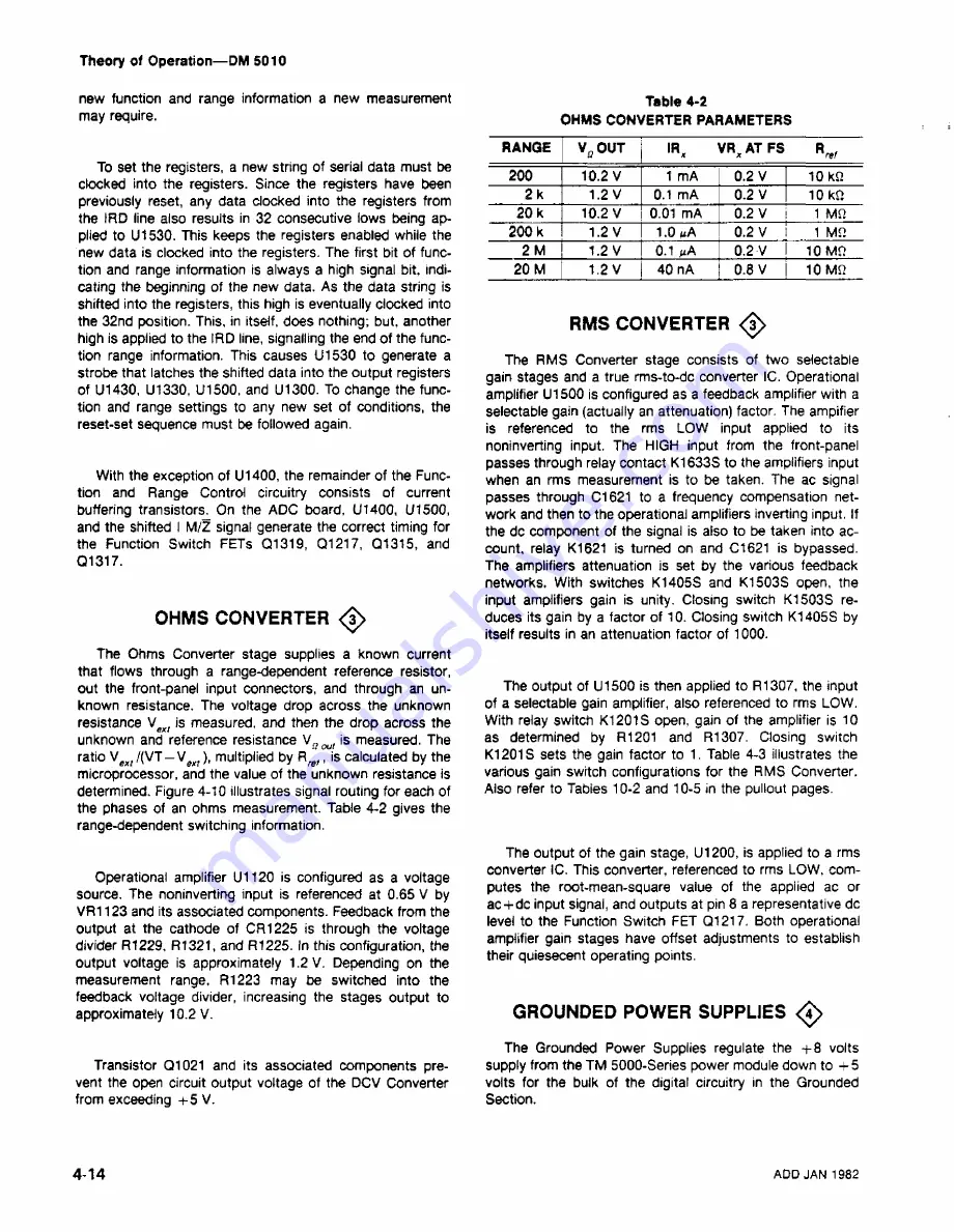
an ohms measurement. Table 4-2 gives the
range-dependent switching information.
Operational amplifier
U1120 is configured as a voltage
source.
The noninverting
input is referenced at 0.65 V by
VR1
123 and its associated components. Feedback from the
output at
the cathode of CR1225 is through the voltage
divider R1229, R1321, and R1225.
In this configuration,
the
output
voltage is approximately 1.2 V. Depending on the
measurement
range,
R1223 may be switched into the
feedback voltage divider,
increasing the stages output
to
approximately
10.2 V.
Transistor
Q1021 and its associated components pre
vent
the open
circuit output voltage of the DCV Converter
from exceeding
+5 V.
Table
4-2
OHMS
CONVERTER PARAMETERS
RANGE
V^OUT
/Rx
AT FS
200
10.2 V
1
mA
0.2 V
10 kΩ
2k
1.2
V
0.1 mA
0.2 V
10 kΩ
20
k
10.2 V
0.01
mA
0.2 V
1
MΩ
200 k
1.2 V
1.0
µA
0.2 V
1
MΩ
2 M
1.2
V
0.1 µA
0.2 V
10 MΩ
20 M
1.2 V
40
nA
0.8
V
10 MΩ
RMS
CONVERTER
<3>
The RMS Converter stage consists of two
selectable
gain stages
and a true rms-to-dc converter IC. Operational
amplifier U1500 is configured as a feedback amplifier with a
selectable gain (actually
an attenuation) factor. The ampifier
is
referenced to the rms LOW input applied to its
noninverting input.
The HIGH input
from the front-panel
passes
through relay contact
K1633S to the
amplifiers input
when
an
rms measurement
is to be taken. The ac signal
passes
through C1621 to a frequency compensation net
work and
then to the operational amplifiers inverting input. If
the
de component of the signal is also to be taken into ac
count, relay K1621 is
turned on and C1621 is bypassed.
The
amplifiers attenuation is set by the various feedback
networks.
With switches
K1405S and K1503S open, the
input amplifiers gain is unity.
Closing switch K1503S re
duces its gain by
a factor of 10. Closing switch
K1405S by
itself results
in
an attenuation factor of 1000.
The output of U1500 is then applied to R1307, the input
of
a selectable
gain amplifier, also
referenced to rms LOW.
With
relay
switch
K1201S open, gain of the amplifier is 10
as determined by
R1201 and R1307. Closing switch
K1201S sets the gain factor to
1. Table 4-3 illustrates the
various gain
switch configurations for the
RMS Converter.
Also
refer to Tables
10-2
and 10-5
in the pullout pages.
The
output of the gain stage,
U1200, is applied to a rms
converter IC.
This converter, referenced to rms LOW, com
putes
the root-mean-square value
of the applied ac or
ac
+
dc
input signal, and outputs at
pin 8 a representative de
level
to the
Function Switch FET Q1217. Both operational
amplifier
gain
stages have offset adjustments to establish
their
quiesecent operating points.
GROUNDED
POWER
SUPPLIES
<4>
The Grounded Power Supplies
regulate the
+8 volts
supply
from
the TM 5000-Series power module down to +5
volts
for
the bulk of
the digital circuitry in the Grounded
Section.
4-14
ADD
JAN
1982
Содержание DM 5010
Страница 14: ...DM 5010 2994 00 DM 5010 Programmable Digital Multimeter xii ADD JUL 1986...
Страница 27: ...Operating Instructions DM 5010 2994 03 Fig 2 3 DM 5010 front panel controls and connectors 2 3...
Страница 38: ......
Страница 40: ...Programming DM 5010 2994 07 Fig 3 1 instrument commands and relationship to front panel controls 3 2...
Страница 101: ...Theory of Operation DM 5010 SOURCE ACCEPTOR 2874 1 50A Fig 4 15 GP B Handshake flowchart ADD JAN 1982 4 27...
Страница 134: ......
Страница 208: ......
Страница 222: ......
Страница 250: ......
Страница 251: ...Section 8 DM 5010 OPTIONS No options are available 8 1...
Страница 252: ......
Страница 270: ......
Страница 272: ...DM 5010 2994 37 Fig 10 2 Location of DM 5010 adjustments and test points...
Страница 273: ......
Страница 274: ......
Страница 275: ......
Страница 276: ...DM 5010 2994 112 DM 5010 BLOCK DIAGRAM...
Страница 281: ......
Страница 282: ......
Страница 291: ......
Страница 293: ......
Страница 294: ......
Страница 297: ......
Страница 298: ......
Страница 303: ......
Страница 304: ...I...
Страница 305: ......
Страница 310: ......
Страница 311: ......
Страница 315: ......
Страница 318: ......
Страница 321: ......
Страница 323: ......
Страница 326: ......
Страница 332: ...2994 57...
Страница 334: ......
Страница 335: ......
Страница 336: ......
Страница 337: ...63 REV JUN 1986...
Страница 338: ...FIG 1 EXPLODED DM 5010...
Страница 339: ......
Страница 340: ......
Страница 341: ......
Страница 347: ......


