background image


Copyright © Siemens AG 2010. All rights reserved.                  

Page


24


ERTEC 400 Manual 

Technical data subject to change                                                                                                                           

Version 1.2.2


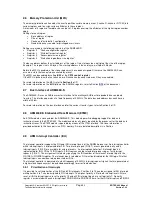
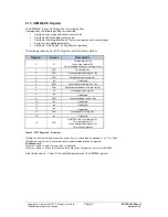
to FIQPR7 are for the FIQ interrupts. A priority must not be assigned more than once. The interrupt control logic 
does not check for assignment of identical priorities. All interrupt requests with a lower or equal priority can be 
blocked at any time in the IRQ priority resolver by assigning a priority in the LOCKREG register. If an interrupt that 
is to be blocked is requested at the same time as the write access to the LOCKREG register, an IRQ signal is 
output. However, the signal is revoked after two clock cycles. If an acknowledgement is to be generated 
nonetheless, the transferred interrupt vector is the default vector.  

2.9.2 

Trigger Modes 

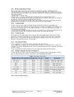
There are two modes available for each interrupt input: “edge-triggered“ and "level-triggered“. 
The trigger type is defined by means of the assigned bit in the TRIGREG register. For the “Edge-triggered” mode 
setting, differentiation can be made between a positive and negative edge evaluation. This is made in the 
EDGEREG register. “Edge-triggered” with positive edge is the default mode assignment for all interrupts. “High” is 
the active level in the “level-triggered" mode. 
The interrupt input signal must be present for at least one clock cycle in “edge-triggered” mode. The input signal 
must be present up until confirmation of the ARM946E-S CPU in "level-triggered" mode. Shorter signals result in 
loss of the event.  

2.9.3 

Masking the Interrupt Inputs 

Each IRQ interrupt can be enabled or disabled individually. The MASKREG register is available for this purpose. 
The interrupt mask acts only after the IRREG interrupt request register. That is, an interrupt is entered in the 
IRREG register in spite of the block in the MASKREG register. After a reset, all mask bits are set and, thus, all 
interrupts are disabled. At a higher level, all IRQ interrupts can be disabled globally via a command. When IRQ 
interrupts are enabled globally via a command, only those IRQ interrupts that are enabled by the corresponding 
mask bit in the MASKREG register are enabled. 
For the FIQ interrupts, only selective masking by the mask bits in the FIQ_MASKREG register is possible. After a 
reset, all FIQ interrupts are disabled. A detected FIQ interrupt request is entered in the FIQ interrupt request 
register. If the interrupt is enabled in the mask register, processing takes place in the priority logic. If the interrupt 
request is accepted by the ARM946 CPU and an entry is made in the in-service request register (ISR), the 
corresponding bit is reset in the IRREG register. Each bit that is set in the IRREG register can be deleted via 
software. For this purpose, the number of the bit to be reset in the IRCLVEC register is transferred to the interrupt 
controller. 

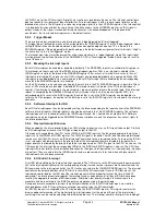
2.9.4 

Software Interrupts for IRQ 

Each IRQ interrupt request can be triggered by setting the bit corresponding to the input channel in the SWIRREG 
software interrupt register. Multiple requests can also be entered in the 16-bit SWIRREG register. The software 
interrupt requests are received directly in the IRREG register and, thus, treated like a hardware IRQ. Software 
interrupts can only be triggered by the ARM946E-S processor because only this processor has access rights to 
the interrupt controller.  

2.9.5 

Nested Interrupt Structure 

When enabled by the interrupt priority logic, an IRQ interrupt request causes an IRQ signal to be output. Similarly, 
an FIQ interrupt request causes the FIQ signal to be output to the CPU. 
If the request is accepted by the CPU (in the IRQACK or FIQACK register), the bit corresponding to the physical 
input is set in the ISREG or FIQISR register. The IRQ/FIQ signal is revoked. The ISR bit of the accepted interrupt 
remains set until the CPU returns an "End-of-interrupt" command to the interrupt controller. As long as the ISR bit 
is set, interrupts with lower priority in the priority logic of the interrupt controller are disabled. Interrupts with a 
higher priority are allowed by the priority logic to pass and generate an IRQ/FIQ signal to the CPU. As soon as the 
CPU accepts this interrupt, the corresponding ISR bit in the ISREG or FIQISR register is also set. The CPU then 
interrupts the lower-priority interrupt routine and executes the higher interrupt routine first. Lower-priority interrupts 
are not lost. They are entered in the IRREG register and are processed at a later time when all higher-priority 
interrupt routines have been executed. 

2.9.6 

EOI End-Of-Interrupt 

A set ISR bit is deleted by the End-of-Interrupt command. The CPU must use the EOI command to communicate 
this to the interrupt controller after the corresponding interrupt service routine is processed. To communicate the 
EOI command to the interrupt controller, the CPU writes any value to the IRQEND/FIQEND register. The interrupt 
controller autonomously decides which ISR bit is reset with the EOI command. If several ISR bits are set, the 
interrupt controller deletes the ISR bit of the interrupt request with the highest priority at the time of the EOI 
command. The interrupt controller regards the interrupt cycle as ended when all of the set ISR bits have been 
reset by the appropriate number of EOI commands. Afterwards, low priority interrupts that occurred in the 
meantime and were entered in the IRREG register can be processed in the priority logic. 
During one or more accepted interrupts, the priority distribution of the IRQ/FIQ interrupt inputs must not be 
changed because the ICU can otherwise no longer correctly assign the EOI commands.  
An IRQ/FIQ request is accepted by the CPU by reading the IRVEC/FIVEQ register. This register contains the 
binary-coded vector number of the highest priority interrupt request at the moment. Each of the two interrupt 
vector registers can be referenced using two different addresses. The interrupt controller interprets the reading of 

Содержание Ertec 400

Страница 1: ...Copyright Siemens AG 2010 All rights reserved Page 1 ERTEC 400 Manual Technical data subject to change Version 1 2 2 ERTEC 400 Enhanced Real Time Ethernet Controller Manual ...

Страница 2: ... reviewed regularly Necessary corrections are included in subsequent editions Suggestions for improvement are welcomed Copyright Siemens AG 2010 All rights reserved The reproduction transmission or use of this document or its contents is not permitted without express written authority Offenders will be liable for damages All rights including rights created by patent grant or registration of a util...

Страница 3: ...your own PROFINET IO device hardware The manual serves as a reference for software developers The address areas and register contents are described in detail for all function groups Structure of this Manual o Section 1 Overview of the architecture and the individual function groups of the ERTEC 400 o Section 2 ARM946E S processor systems o Section 3 Bus system of the ERTEC 400 o Section 4 I O of t...

Страница 4: ... the end of the manual Additional Support If you have questions regarding use of the described block that are not addressed in the documentation please contact your Siemens representative Please send your written questions comments and suggestions regarding the manual to the hotline via the e mail address indicated above In addition you can receive general information current product information F...

Страница 5: ...errupts 23 2 9 2 Trigger Modes 24 2 9 3 Masking the Interrupt Inputs 24 2 9 4 Software Interrupts for IRQ 24 2 9 5 Nested Interrupt Structure 24 2 9 6 EOI End Of Interrupt 24 2 9 7 IRQ Interrupt Sources 25 2 9 8 FIQ Interrupt Sources 25 2 9 9 IRQ Interrupts as FIQ Interrupt Sources 25 2 9 10 Interrupt Control Register 26 2 9 11 ICU Register Description 27 2 10 ARM946E S Register 31 3 Bus System of...

Страница 6: ...PCI bridge reset 66 5 2 5 Actions when HW Reset is Active 66 5 3 Address Space and Timeout Monitoring 67 5 3 1 AHB Bus Monitoring 67 5 3 2 APB Bus Monitoring 67 5 3 3 EMIF Monitoring 67 5 3 4 PCI Slave Monitoring 67 6 External Memory Interface EMIF 69 6 1 Address Assignment of EMIF Registers 70 6 2 EMIF Register Description 70 7 Local Bus Unit LBU 74 7 1 Page Range Setting 75 7 2 Page Offset Setti...

Страница 7: ... 92 9 1 Memory Partitioning of the ERTEC 400 92 9 2 Detailed Memory Description 93 10 Test and Debugging 95 10 1 ETM9 Embedded Trace Macrocell 95 10 1 1 Trace Modes 95 10 1 2 Features of the ETM9 Module 95 10 1 3 ETM9 Registers 95 10 2 Trace Interface 96 10 3 JTAG Interface 96 10 4 Debugging via UART1 96 11 Miscellaneous 97 11 1 Acronyms Glossary 97 11 2 References 98 ...

Страница 8: ...gister 27 Table 5 CP15 Registers Overview 31 Table 6 Overview of AHB Master Slave Access 32 Table 7 Access Type and Data Bit Width of I O 33 Table 8 Selection of Download Source 34 Table 9 Overview of GPIO Registers 35 Table 10 Overview of Timer Registers 38 Table 11 Overview of F Timer Registers 42 Table 12 Overview of WD Registers 44 Table 13 Baud Rates for UART at FUARTCLK 50 MHz 47 Table 14 Ov...

Страница 9: ...ns of the ERTEC 400 Interface module for high accuracy closed loop drive control even for PC based systems Distributed I O with real time Ethernet interfacing PROFINET RT and IRT functionality 1 2 Features of the ERTEC 400 The ERTEC 400 is a high performance Ethernet controller with integrated function groups High performance ARM946 processor with D cache I cache D TCM memory Multilayer AHB bus ma...

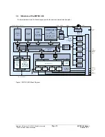
Страница 10: ...Byte Slave 2 x UART SPI Interface 2 x Timer Watchdog F Timer 7 ARM9 clock 50MHz 100MHz 1 1 12 5MHz SC Bus 50MHz MC Bus 50MHz 32 Bit 32 Bit 4 Port Switch Switch Control K SRAM 192 kByte Ethernet Port1 Ethernet Port2 Ethernet Port3 Ethernet Port4 32 7 Slave JTAG Debug Ports serielle SS SPI Watch dog IRT PLL Interface 7 7 RMII Interface AHB Wrapper Slave Master Slave Slave Slave Slave Boot ROM Slave ...

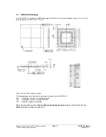
Страница 11: ... pins is 0 8 mm The package dimensions are 19 mm x 19 mm Figure 2 ERTEC 400 Package Description The following documents contain the soldering instructions for the ERTEC 400 10 Soldering instructions for lead based block 11 Soldering instructions for lead free block 12 Code description for soldering When working with modules always take precautionary measures against electrostatic charge ESD Electr...

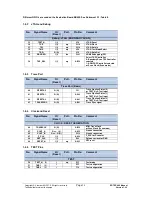
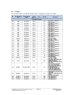
Страница 12: ...I up AA18 GPIO or UART1 or ETM 13 GPIO12 CTS1_N ETMEXTOUT B I O I up W13 GPIO or UART1 or ETM 14 GPIO13 TXD2 B O I up V15 GPIO or UART2 15 GPIO14 RXD2 B I I up U15 GPIO or UART2 16 GPIO15 DCD2_N WDOUT0_N B I O I up W16 GPIO or UART2 or watchdog 17 GPIO16 DSR2_N SSPCTLOE ETMEXTIN1 B I O I I up AB14 GPIO or UART2 or SPI or ETM 18 GPIO17 CTS2_N SSPOE Reserved B I O O I up AA14 GPIO or UART2 or SPI 19...

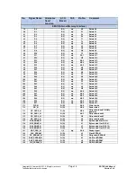
Страница 13: ...3 Trace Port No Signal Name I O Reset Pull Pin No Comment Trace Port Basic 40 PIPESTA0 O O Y21 Trace Pipeline Status 0 or TEST_N 0 Test input 41 PIPESTA1 O O AA22 Trace Pipeline Status 1 or TEST_N 0 Test input 42 PIPESTA2 O O AA21 Trace Pipeline Status 2 or TEST_N 0 Test input 43 TRACESYNC O O AB21 Trace Sync signal 1 5 4 Clock and Reset No Signal Name I O Reset Pull Pin No Comment CLOCK RESET GEN...

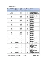
Страница 14: ...RAM Address 6 64 A9 O O G1 Address bit 9 SDRAM Address 7 65 A10 O O H2 Address bit 10 SDRAM Address 8 66 A11 O O H1 Address bit 11 SDRAM Address 9 67 A12 O O J2 Address bit 12 SDRAM Address 10 68 A13 O O J1 Address bit 13 SDRAM Address 11 69 A14 O O E4 Address bit 14 SDRAM Address 12 70 A15 O O F5 Address bit 15 71 A16 BOOT0 1 O I F4 Address bit 16 ERTEC 400 boot mode ext PU PD necessary 72 A17 BO...

Страница 15: ... up R6 Data bit 20 100 D21 B I up R4 Data bit 21 101 D22 B I up R5 Data bit 22 102 D23 B I up T5 Data bit 23 103 D24 B I up V4 Data bit 24 104 D25 B I up W5 Data bit 25 105 D26 B I up AA4 Data bit 26 106 D27 B I up AB4 Data bit 27 107 D28 B I up AA5 Data bit 28 108 D29 B I up AB5 Data bit 29 109 D30 B I up AA6 Data bit 30 110 D31 B I up AB6 Data bit 31 111 WR_N O O AA9 Write strobe 112 RD_N O O AB...

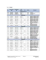
Страница 16: ...ess Data Bit 8 LBU Data Bit 8 137 AD09 LBU_DB09 B B I D8 PCI Address Data Bit 9 LBU Data Bit 9 138 AD10 LBU_DB10 B B I B6 PCI Address Data Bit 10 LBU Data Bit 10 139 AD11 LBU_DB11 B B I E8 PCI Address Data Bit 11 LBU Data Bit 11 140 AD12 LBU_DB12 B B I A6 PCI Address Data Bit 12 LBU Data Bit 12 141 AD13 LBU_DB13 B B I E9 PCI Address Data Bit 13 LBU Data Bit 13 142 AD14 LBU_DB14 B B I B7 PCI Addres...

Страница 17: ...BU_AB16 B I I F14 PCI Address Data Bit 24 LBU Address Bit 16 165 AD25 LBU_AB17 B I I B16 PCI Address Data Bit 25 LBU Address Bit 17 166 AD26 LBU_AB18 B I I E14 PCI Address Data Bit 26 LBU Address Bit 18 167 AD27 LBU_AB19 B I I A17 PCI Address Data Bit 27 LBU Address Bit 19 168 AD28 LBU_AB20 B I I F15 PCI Address Data Bit 28 LBU Address Bit 20 169 AD29 LBU_SEG_0 B I I B17 PCI Address Data Bit 29 LB...

Страница 18: ...1 TXD_P1 1 TXD_P0 3 O O O L21 RMII Transmit data Port 1 Bit 1 MII Transmit data Port 0 Bit 3 192 RXD_P1 0 RXD_P0 2 I I I dn K21 RMII Receive data Port 1 Bit 0 MII Receive data Port 0 Bit 2 193 RXD_P1 1 RXD_P0 3 I I I dn J21 RMII Receive data Port 1 Bit 1 MII Receive data Port 0 Bit 3 194 TX_EN_P1 TX_ERR_P0 O O O M19 RMII Transmit enable Port 1 MII Transmit Error Port0 195 CRS_DV_P1 RX_DV_P0 I I I ...

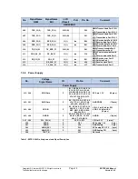
Страница 19: ... dn E21 RMII Receive error Port 3 MII Collision Port 1 213 RX_CLK_P1 I I I dn H18 MII Receive clock Port 1 214 TX_CLK_P1 I I I dn J17 MII Transmit clock Port 1 1 5 9 Power Supply No Voltage Signal Name I O Pin No Comment Power Supply 215 244 VDD Core P B11 D6 D9 D15 E5 E18 E19 F6 F17 H4 J19 K4 L19 M4 N5 N19 P4 P18 R18 U4 U6 U17 V5 V14 V18 W7 W8 W14 W15 W17 SV Core 1 5 V 30 pins 245 261 GND Core P ...

Страница 20: ... the active RESET phase After a reset these pins are available as normal function pins 3 The TMC1 and TMC2 test pins are shorted to ground during operation TEST_N can remain open 4 PCI mode The P5V_PCI pins connect to PCI supply pins V IO see PCI Spec LBU mode The P5V_PCI pins connect to VDD IO 5 The GPIOs 31 0 PCI LBU pins and RMII MII pins can contain different functions Depending on the selecte...

Страница 21: ...d on 1 and 2 2 1 Structure of ARM946E S An ARM946E S processor system is used The figure below shows the structure of the processor In addition to the processor core the system contains one data cache one instruction cache a memory protection unit MPU a system control coprocessor and a tightly coupled memory The processor system has an interface to the integrated AHB bus Figure 3 Structure of ARM9...

Страница 22: ...e user to lock the contents of the cache segments LOCK This function enables the command set for fast routines to be maintained permanently in the instruction cache This mechanism can only be implemented on a segment specific basis in the ARM946E S Both caches are locked after a reset The caches can be enabled only if the memory protection unit is enabled at the same time The I cache can be enable...

Страница 23: ...information on the bus interface and for the various transfer types refer to Section 6 of 1 2 8 ARM946E S Embedded Trace Macrocell ETM9 An ETM9 module is connected at the ARM946E S This module permits debugging support for data and instruction traces in the ERTEC 400 The module contains all signals required by the processor for the data and instruction traces The ETM9 module is operated by means o...

Страница 24: ...upt request can be triggered by setting the bit corresponding to the input channel in the SWIRREG software interrupt register Multiple requests can also be entered in the 16 bit SWIRREG register The software interrupt requests are received directly in the IRREG register and thus treated like a hardware IRQ Software interrupts can only be triggered by the ARM946E S processor because only this proce...

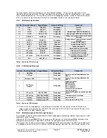
Страница 25: ...5 PCI AHB_INT_L Rising edge AHB PCI bridge Table 2 Overview of IRQ Interrupts 2 9 8 FIQ Interrupt Sources Int No Function Block Signal Name Default Setting Comment 0 Watchdog Rising edge 1 APB bus Rising edge Access to non existing address at the APB 1 2 Multilayer AHB Rising edge Access to non existing address at the AHB 1 3 PLL Status Register Rising edge Group interrupt of EMIF I O QVZ PCI Slav...

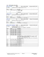
Страница 26: ...ytes R W 0x00000007 FIQ priority register on input FIQ0 of the FIQ interrupt controller FIQPR1 0x0030 4 bytes R W 0x00000007 FIQ priority register on input FIQ1 of the FIQ interrupt controller FIQPR2 0x0034 4 bytes R W 0x00000007 FIQ priority register on input FIQ2 of the FIQ interrupt controller FIQPR3 0x0038 4 bytes R W 0x00000007 FIQ priority register on input FIQ3 of the FIQ interrupt controll...

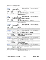
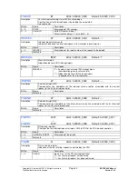
Страница 27: ...cking interrupt requests of lower and equal priority Bit No Name Description 3 0 LOCKPRIO Binary code of lock priority 7 LOCKENABLE 0 Lock inactive 1 Lock active FIQ1SREG R W Addr 0x5000_000C Default 0x0000_0000 Description Fast interrupt request 1 select register Declaration of an IRQ input as FIQ6 input FIQ6 on FIQ interrupt controller Bit No Name Description 3 0 FIQ1SREG Number of the input to ...

Страница 28: ...isable for all IRQ interrupt inputs independent of the interrupt mask IRQEND W Addr 0x5000_0024 Default Description End of interrupt IRQ Communicates the completion of the interrupt service routine associated with the current request to the IRQ interrupt controller Bit No Name Description Not used FIQEND W Addr 0x5000_0028 Default Description End of interrupt FIQ Communicates the completion of the...

Страница 29: ...pt request active MASKREG R W Addr 0x5000_005C Default 0x0000_FFFF Description Interrupt mask register Enable disable of interrupt inputs Bit No Name Description 15 0 MASKREG Interrupt input 0 to 15 0 Interrupt input enabled 1 Interrupt input disabled ISREG R Addr 0x5000_0060 Default 0x0000_0000 Description In service register Indication of the interrupt requests confirmed by the CPU Bit No Name D...

Страница 30: ...cification of interrupt requests Bit No Name Description 15 0 SWIRREG Interrupt input 0 to 15 0 No interrupt request 1 Set interrupt request PRIOREG 0 R W Addr 0x5000_0070 Default 0x0000_000F PRIOREG 15 R W Addr 0x5000_00AC Default 0x0000_000F Description Priority register Specification of priority of an interrupt request at the associated input Bit No Name Description 3 0 PRIOREG Binary code of t...

Страница 31: ...nfiguration register 2 3 W R Write buffer control register 4 xxx Undefined 5 W R Access permission register 2 6 W R Protection region base size register 2 7 W Cache operation register 8 xxx Undefined 9 W R Cache lockdown register 2 10 xxx Undefined 11 xxx Undefined 12 xxx Undefined 13 W R Trace process ID register 14 xxx Undefined 15 W R RAM TAG BIST test register 1 Test state register 1 Cache deb...

Страница 32: ...ously Each of the AHB arbiters uses the same arbitration procedure Round robin is specified Alternatively a fixed priority assignment of the AHB master can be set through assignment of the ARB_MODE bit in the M_LOCK_CNTL system control register Fixed priority assignment should be avoided due to the dynamic sequences on the multilayer AHB bus The round robin arbitration procedure prevents mutual bl...

Страница 33: ... 0 Function Block 32 bit Timer F counter Watchdog System control register Boot_Rom 8 bit 8 bit 8 bit 8 bit 16 bit 16 bit 32 bit GPIO 16 bit SPI 8 bit UART1 2 Table 7 Access Type and Data Bit Width of I O Accesses to non decoded out memory or register areas trigger an FIQ interrupt Access by a generated Ready signal from the APB address decoder is closed Write accesses do not affect the system Read...

Страница 34: ...I compatible Data Flash e g AT45DB011B GPIO 23 1 SPI compatible EEPROM e g AT25HP256 The serial protocols by Motorola Texas Instruments and NSC are supported in principle Caution If an image that is booted via SPI interface does not contain any Read Write data i e only Read Only data the checksum is not calculated properly and the image is not started Workaround Define at least one global variable...

Страница 35: ...t inputs They are connected at the IRQ interrupt controller of the ARM946 An interrupt can be generated only with an active High input level rising edge or falling edge for parameter assignment refer to Section 2 9 11 The following figure shows the structure of a GPIO pin as a standard I O function or as an alternative function GPIO i GPIO IN GPIO OUT i Alternate Function 1 2 3 if Input Alternate ...

Страница 36: ...on register for GPIO Port 0 to 15 Function assignment 00 Function 0 01 Function 1 10 Function 2 11 Function 3 Bit No Name Description 1 0 GPIO0_PORT_MODE Port GPIO 0 3 2 GPIO1_PORT_MODE Port GPIO 1 5 4 GPIO2_PORT_MODE Port GPIO 2 7 6 GPIO3_PORT_MODE Port GPIO 3 9 8 GPIO4_PORT_MODE Port GPIO 4 11 10 GPIO5_PORT_MODE Port GPIO 5 13 12 GPIO6_PORT_MODE Port GPIO 6 15 14 GPIO7_PORT_MODE Port GPIO 7 17 1...

Страница 37: ... for bits 7 6 13 12 GPIO22_PORT_MODE Port GPIO 22 See note for bits 7 6 15 14 GPIO23_PORT_MODE Port GPIO 23 17 16 GPIO24_PORT_MODE Port GPIO 24 19 18 GPIO25_PORT_MODE Port GPIO 25 21 20 GPIO26_PORT_MODE Port GPIO 26 23 22 GPIO27_PORT_MODE Port GPIO 27 25 24 GPIO28_PORT_MODE Port GPIO 28 27 26 GPIO29_PORT_MODE Port GPIO 29 29 28 GPIO30_PORT_MODE Port GPIO 30 31 30 GPIO31_PORT_MODE Port GPIO 31 4 3 ...

Страница 38: ... evaluation 4 3 3 Timer Prescaler An 8 bit prescaler is available for each timer Settings can be made independently for each prescaler Each prescaler has its own 8 bit reload register If the reload value or starting value of the prescaler is 0 prescaling does not occur The current prescaler value cannot be read out In addition there are no status bits for the prescalers The prescalers always run i...

Страница 39: ...elevant can be read write accessed 4 Reserved Not relevant read 0 5 Status Timer status writing is ignored 0 Timer has not expired 1 Timer has expired count is 0 and Run xStop Bit 0 1 Note This bit can only be read as 1 if Run xStop Bit 0 is active 1 31 6 Reserved Not relevant read 0 Important note The bits designated with are not applicable if the timers are cascaded See CTRL_STAT1 CTRL_STAT1 R W...

Страница 40: ... of prescaler 0 with the reload register value 0 Not relevant 1 Timer is loaded with the value of the reload register While this bit can be read back the trigger only has an effect at the instant of writing The prescaler is loaded independently of the status of Run xStop_V0 2 Run xStop_V1 Stop start of prescaler 1 0 Prescaler 1 is stopped 1 Prescaler 1 is running 3 Load_V1 Trigger loading of presc...

Страница 41: ...ses are generated in a series connected edge detection All flip flops run at the APB clock of 50 MHz The F_COUNTER_VAL register is reset using an asynchronous block reset or by writing the value 0x XXXX 55AA X means don t care to the F counter register FCOUNT_RES The next count pulse sets the counter to 0xFFFF FFFF and the counter is decremented at each additional count pulse The FCOUNT_RES regist...

Страница 42: ...es W 0x00000000 Reset register for F counter Table 11 Overview of F Timer Registers 4 4 2 F Timer Register Description F COUNTER VAL R Addr 0x4000_2700 Default 0x0000_0000 Description Timer value of F counter Bit No Name Description 31 0 F CNT VAL 31 0 Timer value of F timer F COUNTER RES W Addr 0x4000_2704 Default 0x0000_0000 Description Reset register for F counters A reset of the F counter is p...

Страница 43: ... 0 are set to 0 The count values of the watchdog timers can also be read When watchdog timer 1 is read bits 35 4 are read out The status of the two watchdog timers can be read out in the CTRL STATUS register 4 5 3 Watchdog Interrupt The WDINT interrupt of the watchdog is routed to the FIQ interrupt controller The interrupt is only active High if watchdog timer 0 is in RUN mode and watchdog timer 0...

Страница 44: ... Register Description CTRL STATUS R W Addr 0x4000_2100 Default 0x0000_0000 Description Control status register Configuration and control bits for the watchdog Bit No Name Description 0 Run xStop_V0 Enable disable watchdog counter 0 0 Watchdog counter 0 disabled 1 Watchdog counter 0 enabled Note If this bit 0 the WDOUT0_n output of the ERTEC 400 is active 0 the interrupt of the watchdog WDINT is 0 ...

Страница 45: ... Addr 0x4000_210C Default 0x0000_FFFF Description Reload register 1_Low Reload value for bits 19 4 of watchdog counter 1 Bit No Name Description 15 0 Reload1 19 4 Reload value for bits 19 4 of watchdog counter 1 31 16 Key bits Key bits for writing to this register read 0 If bits 31 16 9876h writing of bits 0 15 of this register has an effect otherwise no effect RELD1_HIGH R W Addr 0x4000_2110 Defa...

Страница 46: ... the ERTEC 400 Transmit cable 1 per UART TXD1 TXD2 Receive cable 1 per UART RXD1 RXD2 Handshake 3 per UART DCD1_N DCD2_N CTS1_N CTS2_N DSR1_N DSR2_N Both UARTs are implemented as ARM Prime Cell TM PL010 macros These are similar to standard UART 16C550 For a detailed description refer to 5 The figure below shows the structure of the UART Figure 7 Block Diagram of UART The UARTs differ from standard...

Страница 47: ...I BAUDDIV BR EP 115200 26 115740 0 47 76800 40 76219 0 76 57600 53 57870 0 47 38400 80 38580 0 47 19200 162 19171 0 15 14400 216 14400 9 0 006 9600 325 9585 9 0 15 2400 1301 2400 15 0 006 1200 2603 1200 077 0 006 110 28408 110 0004 0 0003 Table 13 Baud Rates for UART at FUARTCLK 50 MHz UART 1 can also be used as a BOOT medium if for example functions from an external PC are to be loaded to the ERT...

Страница 48: ...x009C 0x00FF Reserved for future extension Table 14 Overview of UART 1 2 Registers 4 6 2 UART 1 2 Register Description UARTDR 1 R W Addr 0x4000_2300 Default 0x UARTDR 2 R W Addr 0x4000_2400 Default 0x Description UART data registers Bit No Name Description 7 0 WRITE If FIFO is enabled the written data are entered in the FIFO If FIFO is disabled the written data are entered in the Transmit holding ...

Страница 49: ... generation Even parity select 0 Odd parity 0 for check and generation 3 STP2 Two stop bit select 1 Two stop bits are appended at the end of the frame when sending Two stop bit select 0 One stop bit is appended at the end of the frame when sending 4 FEN FIFO enable 1 FIFO modes for sending and receiving are enabled FIFO enable 0 FIFO is disabled Sending receiving is then performed via 1 byte holdi...

Страница 50: ...1 Transmit interrupt is enabled 6 RTIE Receive timeout interrupt enable 1 Receive timeout interrupt is enabled 7 LBE Loop back enable UARTFR 1 R Addr 0x4000_2318 Default 0x9 UARTFR 2 R Addr 0x4000_2418 Default 0x9 Description UART flag registers Bit No Name Description 0 CTS Clear To Send This bit is the inverse signal of UART input CTS 1 DSR Data Set Ready This bit is the inverse signal of UART i...

Страница 51: ...2 TIS Read Transmit Interrupt Status This bit is set if UARTTXINTR is active 3 RTIS Read Receive Timeout Interrupt Status This bit is set if UARTRTINTR is active 7 4 Read Reserved Value is undefined 7 0 Write Writing to this register deletes the MIS bit irrespective of the value written UARTILPR 1 R W Addr 0x4000_2320 Default 0x00 UARTILPR 2 R W Addr 0x4000_2420 Default 0x00 Description UART IrDA ...

Страница 52: ...EC 400 Transmit cable 1 SSPTXD Receive cable 1 SSPRXD Clock cable 2 SCLKIN SCLKOUT Enables 2 SSPCTLOE SSPOE SFRs 2 SFRMIN SFRMOUT The SPI interface is implemented as ARM Prime Cell TM PL021 macros For a detailed description refer to 6 The figure below shows the structure of the SPI macro Figure 8 Block Diagram of SPI The SPI interface supports the following modes Motorola SPI compatible mode Texas...

Страница 53: ...nd loading of the program code For BOOT mode with SPI interface the GPIO 22 is used as a chip select signal 4 7 1 Address Assignment of SPI Register The SPI registers are 16 bits in width For read write access of the SPI registers to be meaningful a 16 bit access is required However a byte by byte write operation is not intercepted by the hardware SPI Base Address 0x4000_2200 Register Name Offset ...

Страница 54: ...xpected clock cycle after frame signal has gone to Low 15 8 SCR Serial Clock Rate The serial clock rate is taken for calculation of the Transmit Receive bit rate The calculation formula is as follows FSSPCLK CPSDVSR x 1 SCR SCR 1 to 255 CPSDVSR 2 to 254 for a description refer to SSPCPSR Register SSPCR1 R W Addr 0x4000_2204 Default 0x0000 Description Control register 1 Configuration frame format a...

Страница 55: ...rmat When data are read they are read out correctly from the Receive FIFO SSPSR R Addr 0x4000_220C Default 0x0000 Description SPI status register Bit No Name Description 0 TFE Transmit FIFO empty 0 Transmit FIFO is not empty 1 Transmit FIFO is empty 1 TNF Transmit FIFO not full 0 Transmit FIFO is full 1 Transmit FIFO is not full 2 RNE Receive FIFO not empty 0 Receive FIFO is empty 1 Receive FIFO i...

Страница 56: ...width System Control Registers Base address 0x4000_2600 Register Name Offset Address Address Area Access Default Description ID_REG 0x0000 4 bytes R 0x40260100 ID ERTEC 400 BOOT_REG 0x0004 4 bytes R 0x Boot mode pins Boot 0 2 CONFIG_REG 0x0008 4 bytes R 0x ERTEC 400 config pins Config 0 4 RES_CTRL_REG 0x000C 4 bytes W R 0x00000100 Control register for reset of ERTEC 400 RES_STAT_REG 0x0010 4 bytes...

Страница 57: ...x00000000 Write protection register for ARM9_CTRL 0x0058 76 bytes Reserved Table 16 Overview of System Control Registers 4 8 2 System Control Register Description ID_REG R Addr 0x4000_2600 Default 0x4026_0100 Description Identification of ERTEC 400 Bit No Name Description 31 16 ERTEC400 ID ERTEC 400 identifier 4026h corresponds to the device ID of the AHB PCI bridge 15 8 HW RELEASE HW release 01h ...

Страница 58: ...RES_CTRL_REG has to be written again by the software RES_STAT_REG R Addr 0x4000_2610 Default 0x0000_0004 Description Status register for reset of ERTEC 400 Only the bit of the last reset event occurrence is set The two other bits are reset Bit No Name Description 31 3 Reserved 2 HW_RESET 1 Last reset was a hardware reset 1 SW_RESET 1 Last reset was via a software reset 0 WD_RESET 1 Last reset was ...

Страница 59: ... PLL 0 PLL is unlocked 1 PLL is locked This bit represents the current lock state of the PLL Read access only Note Under very rare conditions in PCI boot mode it is possible that the interrupt bit 4 INT_QVZ_PCI_STATE in register PLL_STAT_REG will be left on after finishing the 1st level boot Workaround To avoid irritations concerning the interrupt causes it is recommended to reset interrupt bit 4 ...

Страница 60: ...scription 31 0 QVZ_AHB_ADR Address QVZ_AHB_CTRL R Addr 0x4000_262C Default 0x0000_0000 Description Control signals of incorrect addressing on multilayer AHB Bit No Name Description 31 7 Reserved 6 4 HBURST HBURST 3 1 HSIZE HSIZE 0 HWRITE HWRITE 0 HREAD 1 HWRITE QVZ_AHB_M R Addr 0x4000_2630 Default 0x0000_0000 Description Master identifier of an incorrect addressing on the multilayer AHB Bit No Nam...

Страница 61: ...1 Request is active PCI_RES_ACK R Addr 0x4000_2640 Default 0x0000_0000 Description Acknowledge register for display of an implemented soft reset request Bit No Name Description 31 1 Reserved 0 PCI_SOFT_RES_ACK Display of implemented soft reset by PCI bridge 0 Request was not implemented 1 Request was implemented MEM_SWAP R W Addr 0x4000_2644 Default 0x0000_0000 Description Memory swapping in Segme...

Страница 62: ...M9_WE register This register can only be changed for debugging purposes Bit No Name Description 31 14 Reserved 13 BIGENDIAN BIGENDIAN read only 12 DISABLE_GATE_THE CLK DisableGateTheClk 1 ARM9 processor clock runs freely 0 ARM9 processor clock is paused by a Wait for Interrupt 11 DBGEN DBGEN Enable of embedded ARM9 debugger 1 Debugger is enabled 0 Debugger is disabled 10 MICEBYPASS MICEBYPASS Bypa...

Страница 63: ...MII RMII RX TX clock MII REF_CLK RMII 25 MHz MII 50 MHz RMII Table 17 Overview of ERTEC 400 Clocks Synchronous clocks CLK_50MHz and CLK_100MHz are used primarily in the ERTEC 400 These clocks are generated with an internal PLL that is in turn supplied by a quartz or oscillator The input clock is selected using the CONFIG0 configuration pin CONFIG0 0 Input clock is fed with a quartz via the CLKP_A ...

Страница 64: ...e AHB clock CLK_50MHz is enabled for the LBU clock supply The clock supply for the LBU is disabled in PCI mode In LBU mode it is recommended that the AHB clock for the PCI bridge be disabled Configuration pin CONFIG2 is used to select PCI or LBU mode CONFIG2 0 LBU mode CONFIG2 1 PCI mode 5 1 4 JTAG Clock Supply The clock supply for the JTAG interface is implemented using the JTAG_CLK pin The frequ...

Страница 65: ...s Hardware reset via external RESET_N pin Software reset via XRES_SOFT bit in the reset control register Watchdog reset via watchdog timer overflow The triggering reset event can be read out in the reset status register 5 2 1 Hardware Reset The external hardware reset circuitry is connected at the RESET_N pin of the ERTEC 400 If the hardware reset is enabled the entire ERTEC 400 circuit except for...

Страница 66: ...g the XRES_PCI_AHB_SOFT bit in the reset control register The PCI bridge side that is clocked with CLK_PCI 33 66 MHz resets the RES_PCI_N output The state of RES_PCI_N can be read in the reset control register The PCI bridge side that is clocked with CLK_50MHz is reset by XRES_PCI_AHB_SOFT software resets In order to ensure a defined state of the PCI bridge through the reset sources indicated abov...

Страница 67: ...in the QVZ_APB_ADR system control register The QVZ_APB_ADR system control register is locked for subsequent address violations until it has been read 5 3 3 EMIF Monitoring In the case of the EMIF the external RDY_PER_N ready signal is monitored In order to enable monitoring Extended_Wait_Mode must be switched on in the Async_Bank_0_Config to Async_Bank_3_Config configuration registers If one of th...

Страница 68: ...ted The slave must continue to wait for signal HSPLIT 1 As long as the signal to the slave is missing all other accesses to the slave must be blocked with an error response According to the AHB specification once the slave outputs HSPLIT 1 access must be repeated However because access is already terminated for the master the data phase can no longer be handled correctly Caution Under very rare co...

Страница 69: ...N WR_N Ready 1 RDY_PER_N DIR 2 DTR_N OE_DRIVER_N SDRAM 5 CLK_SDRAM CS_SDRAM_N RAS_SDRAM_N CAS_SDRAM_N WE_SDRAM_N The SDRAM controller has the following features 16 bit or 32 bit data bus width can be assigned PC100 SDRAM compatible 50 MHz clock frequency A maximum of 256 Mbytes of SDRAM for 32 bit data bus width or A maximum of 128 Mbytes of SDRAM for 16 bit data bus width Supports various SDRAMs ...

Страница 70: ...ming data bus width for access via async interface CS_PER1_N Async_BANK2_Config 0x0018 4 bytes W R 0x3FFFFFF2 Timing data bus width for access via async interface CS_PER2_N Async_BANK3_Config 0x001C 4 bytes W R 0x3FFFFFF2 Timing data bus width for access via async interface CS_PER3_N Extended_Config 0x0020 4 bytes W R 0x03030000 Setting of additional functionalities Table 18 Overview of EMIF Regis...

Страница 71: ... banks in the SDRAM 000 1 bank 001 2 banks 010 4 banks 011 111 Reserved 3 Reserved 2 0 PAGESIZE Page size 000 SDRAM with 8 column address lines 001 SDRAM with 9 column address lines 010 SDRAM with 10 column address lines 011 SDRAM with 11 column address lines 100 111 Reserved Attention Writing to SDRAM_Bank_Config executes the Mode Register Set command on the SDRAM if Bit 29 init_done is set in th...

Страница 72: ... w_su 1 AHB clock cycles between valid address data and chip select and falling edge of the write signal 25 20 W_STROBE Write strobe duration cycles w_strobe 1 AHB clock cycles between falling and rising edges of the write signal 19 17 W_HOLD Write strobe hold cycles w_hold 1 AHB clock cycles between rising edge of the write signal and change of address data and chip select 16 13 R_SU Read strobe ...

Страница 73: ...ta bus After each access to the asynchronous area the data bus is driven actively to 1 at the end of the Hold phase in order to support integrated pull ups 23 20 Reserved 19 TEST_3 Test Mode 3 0 Normal function 1 DTR_N Test Output 18 Reserved 17 16 BURST_LENGTH SDRAM burst length 00 1 01 2 10 Full Page Read INCR_S burst length 4 11 Full Page Read INCR_S burst length 8 15 Reserved 14 TRCD TCD Time ...

Страница 74: ...age The LBU_CS_R_N chip select signal can be used to access the page registers The following settings are possible for each page Access size of a page between 256 bytes and 2 Mbytes with 2 page range register Offset segment of page in 4 Gbyte address area with 2 page offset register Access type data bit width with 1 page control register The ERTEC 400 internal address area is accessed via the LBU_...

Страница 75: ... table above the largest page is 1 Mbyte i Bit 20 The maximum addresses are calculated from Amax 20 1 In this case address cables A 19 0 are required This addressing mechanism results in a mirroring of the specified page size in the total segment 7 2 Page Offset Setting The page offset of each page is set in the PAGEx_OFFSET_HIGH and PAGEx_OFFSET_LOW range registers x 0 to 3 Together the two page ...

Страница 76: ...en the LOW word is read In addition the LOW word is forwarded and the HIGH word is stored temporarily in the LBU A subsequent read access to the HIGH word address outputs the temporarily stored value This ensures consistent reading of 32 bit data on a 16 bit bus In the case of 32 bit write access the LOW word is first stored temporarily in the LBU area When the HIGH word is write accessed a 32 bit...
Страница 77: ...n Min Max tCSRS chip select asserted to read pulse asserted delay 0 ns tARS address valid to read pulse asserted setup time 0 ns tRRE read pulse asserted to ready enabled delay 5 ns 12 ns tRDE read pulse asserted to data enable delay 5 ns 12 ns tRAP ready active pulse width 17 ns 23 ns tRTD ready asserted to data valid delay 5 ns tRCSH read pulse deasserted to chip select deasserted delay 0 ns tRA...

Страница 78: ... Max tCSWS chip select asserted to write pulse asserted delay 0 ns tAWS address valid to write pulse asserted setup time 0 ns tWRE write pulse asserted to ready enabled delay 5 ns 12 ns tWDV write pulse asserted to data valid delay 40 ns tRAP ready active pulse width 17 ns 23 ns tWCSH write pulse deasserted to chip select deasserted delay 0 ns tWAH address valid to write pulse deasserted hold time...

Страница 79: ...WCS write signal deasserted to chip select asserted setup time 2 ns tACS address valid to chip select asserted setup time 0 ns tCRE chip select asserted to ready enabled delay 5 ns 12 ns tCDE chip select asserted to data enable delay 5 ns 12 ns tRAP ready active pulse width 17 ns 23 ns tRTD ready asserted to data valid delay 5 ns tCWH write signal inactive to chip select deasserted hold time 0 ns ...

Страница 80: ...lid enabled to chip select deasserted hold time 0 ns tWR write recovery time 25 ns Table 25 LBU write access timing with common Read Write line 1 The setup time tWCS must be maintained under all circumstances otherwise the LBU unit drives the ERTEC 400 databus The ERTEC 400 has two LBU chip select inputs One for access to the page configuration register LBU_CS_R_N and one to access to the ERTEC 40...

Страница 81: ...ter 1 Low LBU_P1_RG_H 0x0012 2 bytes W R 0x0000 LBU pagex range register 1 High LBU_P1_OF_L 0x0014 2 bytes W R 0x0000 LBU pagex offset register 1 Low LBU_P1_OF_H 0x0016 2 bytes W R 0x0000 LBU pagex offset register 1 High LBU_P1_CFG 0x0018 2 bytes W R 0x0000 LBU configuration register 1 LBU_P2_RG_L 0x0020 2 bytes W R 0x0000 LBU pagex range register 2 Low LBU_P2_RG_H 0x0022 2 bytes W R 0x0000 LBU pa...

Страница 82: ...ite accessible LBU_P0_OF_L W R Addr LBU_CS_R_N 0x04 Default 0x0000_0000 LBU_P1_OF_L W R Addr LBU_CS_R_N 0x14 Default 0x0000_0000 LBU_P2_OF_L W R Addr LBU_CS_R_N 0x24 Default 0x0000_0000 LBU_P3_OF_L W R Addr LBU_CS_R_N 0x34 Default 0x0000_0000 Description Low word of LBU Pagex_Offset_register Bit No Name Description 15 0 Lower 16 bits for offset setting 15 8 are read write accessible 7 0 are read o...

Страница 83: ... cables 11 PAR FRAME_N IRDY_N TRDY_N DEVSEL_N STOP_N IDSEL PERR_N REQ_N GNT_N M66EN PCI bus clock 1 CLOCK_PCI PCI bus reset 1 RES_PCI_N CS for 4 address spaces 4 CBE0_N CBE3_N Interrupt outputs 3 INTA_N INTB_N SERR_N 8 1 PCI Functionality The PCI functions are described in general terms in this section 8 1 1 General Functions of the PCI Interface Compliant with PCI Specification 2 2 Host functiona...

Страница 84: ...oincide for this to happen 1 PCI bridge is used as PCI target AND PCI master 2 ARM initiates read accesses to the memory of the external host as a PCI master 3 External host initiates write accesses to the memory at ERTEC400 EMIF ERTEC400 as PCI target 4 AHB arbiter is set to round robin mode or ARM has the highest priority when the AHB arbiter is set to fixed priority mode The described combinati...

Страница 85: ...ontroller of the ARM946 This enables operation of a mailbox from the PCI host to the ARM946 When PC based systems are linked only INTA_N is used only 1 function of the PCI bridge The INTB_N output is not used When an embedded host processor is linked both INTA_N and INTB_N can be used The local ARM processor is linked via the IRQ0_SP and IRQ1_SP interrupts Both are linked via the internal logic st...

Страница 86: ... is only generated from the PCI bridge address parity error IRT interrupts IRQ0_HP and IRQ_IRT_API_ERR synchronization problems in the IRT API can be enabled according to the setting in the PCI_INT_CNRL system control register Interrupt output SERR_N is a PCI synchronous signal When used the IRQ0_HP and IRQ_IRT_API_ERR interrupts are synchronized to the PCI clock and kept active for the duration o...

Страница 87: ...ther not aligned accesses are rejected with Target Abort Caution In case of subsequent AHB read bursts to the AHB PCI bridge two effects may occur under special cirumstances A Delay of a read burst max 655 4 µs until the discard timer of the AHB PCI bridge elapsed B Data corruption of a read burst The problems occur when all of the following conditions are fulfilled Subsequent read bursts to the A...

Страница 88: ...t be disabled because the PC interface of the ERTEC 400 is only a single function interface However in order for a low priority interrupt to be interrupted by a high priority interrupt from the IRT switch the IRQ0_HP interrupt can be output on the SERR_N output In the case of PC processors this results in an NMI interrupt Optionally IRT interrupt IRQ_IRT_API_ERR can also be placed on the SERR_N ou...

Страница 89: ... enables very simple single master communication to be established between several ERTEC 400s via the PCI bus In the case of local onboard PCI bus systems the IRQ0 HP interrupt high priority IRT interrupt can be switched to the INTB_N output because an independent software structure is provided in this case For consistent non aligned accesses where IRT switch data must be accessed consistency assu...

Страница 90: ...e_ID Vendor_ID R W 0x00000000 0x0044 Subsystem_ID Subsystem_Vendor_ID R W 0x00000000 0x0048 PM_Capability PM_next_item_ptr PM_Capability_id R 0x00020001 0x004C PM_Data PM_CSR_BSE PM_Control_Status R W 0x00000000 0x0050 PCI_Base_Address_Mask_Register0 R W 0x00000000 0x0054 PCI_Base_Address_Mask_Register1 R W 0x00000000 0x0058 PCI_Base_Address_Mask_Register2 R W 0x00000000 0x005C PCI_Base_Address_Ma...

Страница 91: ...ion_Register3 R W 0x00000000 0x00C8 AHB_Base_Address_Translation_Register4 R W 0x00000000 0x00CC AHB_Status_Register AHB_Function_Register R W 0x00000000 0x00D0 Wait_States_Bridge _as_PCI_Target Wait_States_Bridge _PCI_Master Wait_States_Bridge _as_AHB_Slave Wait_States_Bridge _AHB_Master R W 0x00000000 0x00D4 Bridge_Interrupt_Status_Register R 0x00000000 0x00D8 AHB_Interrupt_Enable_Register R W 0...

Страница 92: ...0 0FFF FFFF 0 Internal Boot ROM or internal RAM Internal Boot ROM or internal RAM Internal Boot ROM or internal RAM 1000 0000 1FFF FFFF 1 IRT switch Not used IRT switch 2000 0000 2FFF FFFF 2 EMIF SDRAM EMIF SDRAM EMIF SDRAM 3000 0000 3FFF FFFF 3 EMIF asynchr Memory Area Bank 0 3 EMIF asynchr Memory Area Bank 0 3 EMIF asynchr Memory Area Bank 0 3 4000 0000 4FFF FFFF 4 All APB macros incl boot ROM N...

Страница 93: ...ytes 3200_0000 32FF_FFFF When a smaller device is interfaced mirroring over the entire 16 Mbytes EMIF I O Bank 3 16 Mbytes 3300_0000 33FF_FFFF When a smaller device is interfaced mirroring over the entire 16 Mbytes Not used 3400_0000 3FFF_FFFF 4 Internal boot ROM 8 Kbytes 4000_0000 4000_1FFF 8 Kbytes physical Timer 256 bytes 4000_2000 4000_20FF 32 bytes physical Note2 Watchdog 256 bytes 4000_2100 ...

Страница 94: ...re used 2 4 Mbyte area for unaligned consistent 16 bit accesses to IRT 4 6 Mbyte area for unaligned consistent 32 bit accesses to IRT 6 8 Mbytes is not supported supplies undefined values The 8 Mbyte address area is mirrored 32 times within the 256 Mbytes 2 Memory areas are mirrored according to the following formula Memory size N Physical memory size Physical memory size is limited to values of 2...

Страница 95: ...wing features 4 address comparators 2 data comparators with filter function 4 direct trigger inputs one of which can be connected via a GPIO port 1 trigger output that is also available at the GPIO port for external purposes 8 memory map decoders for decoding the physical address area of the ERTEC 400 1 sequencer 2 counters Supplemental to the ETM specification the 8 MMD regions have been decoded ...

Страница 96: ... In addition to the JTAG interface the DBGREQ and DBGACK signals are available as alternative function pins for debugging Due to the different debuggers an internal pull up resistor at the TRST_N JTAG pin is not included The user has to ensure the proper circuitry for the utilized debugger The standard connector for JTAG interfaces is a 20 pin connector with a pin spacing of 0 1 inch All JTAG pins...

Страница 97: ...ller EMIF External Memory Interface ETM Embedder Trace Macrocell FIQ Fast Interrupt Request GPIO General Purpose Input Output ICE In Circuit Emulator ICU Interrupt Controller Unit IRQ Interrupt Request IRT Isochronous Real Time ITCM Instruction Tightly Coupled Memory JTAG Joint Test Action Group LBU Local Bus Unit MAC Media Access Controller MII Media Independent Interface MPU Memory Protection Un...

Страница 98: ...on Revision 2 0 1999 ARM 5 ARM Prime Cell TM UART PL010 Technical Reference Manual ARM 6 ARM Prime Cell TM Synchronous Serial Port PL021 Technical Reference Manual 7 Embedded Trace Macrocell Architecture Specification ETM_Spec PDF 8 Multi ICE System Design Consideration Applic Note 72 DAI0072A_Multiicedesign Notes PDF 9 IEEE Standard Test Access Port and Boundary Scan Architecture 1149 1 IEEE Boun...

Отзывы: