


Copyright © Siemens AG 2010. All rights reserved.
Page
93
ERTEC 400 Manual
Technical data subject to change
Version 1.2.2
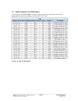
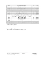
9.2 Detailed Memory Description
The table below presents a detailed description of the memory segments. Mirrored segments should not be used
for addressing to ensure compatible memory expansion at a later date. When a locked I-cache and D-TCM are
used, they can only be addressed by the ARM946E-S and not by PCI or IRT.
When the I-cache is used, it cross-fades the first 4 Kbytes (0-4k) of the memory area. The D-TCM memory can be
placed anywhere in the address space of the ARM946E-S.
Segment
Contents
Size
Address Area
Description
0
Internal Boot ROM or
internal RAM
256 Mbytes
0000_0000 - 0FFF_FFFF
After reset: Boot ROM (8 Kbytes, physical)
After memory swap: internal USER RAM (8
Kbytes, physical)
Note2
1
IRT switch
256 Mbytes
1000_0000 - 1FFF_FFFF
8 Mbytes, physical:
*
0-1 Mbyte for registers
* 1-2 Mbytes for communication RAM (192
Kbytes)
Note1
2
EMIF (SDRAM)
256 Mbytes
2000_0000 - 2FFF_FFFF
When a smaller memory area is used,
mirroring over the entire area
3
EMIF
I/O Bank 0
16 Mbytes
3000_0000 - 30FF_FFFF
When a smaller device is interfaced, mirroring
over the entire 16 Mbytes
EMIF
I/O Bank 1
16 Mbytes
3100_0000 - 31FF_FFFF
When a smaller device is interfaced, mirroring
over the entire 16 Mbytes
EMIF
I/O Bank 2
16 Mbytes
3200_0000 - 32FF_FFFF
When a smaller device is interfaced, mirroring
over the entire 16 Mbytes
EMIF
I/O Bank 3
16 Mbytes
3300_0000 - 33FF_FFFF
When a smaller device is interfaced, mirroring
over the entire 16 Mbytes
Not used
3400_0000 - 3FFF_FFFF
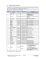
4
Internal boot ROM
8 Kbytes
4000_0000- 4000_1FFF
8 Kbytes, physical
Timer
256 bytes
4000_2000 - 4000_20FF
32 bytes, physical Note2
Watchdog
256 bytes
4000_2100 - 4000_21FF
28 bytes, physical Note2
SPI
256 bytes
4000_2200 - 4000_22FF
256 bytes, physical
UART1
256 bytes
4000_2300 - 4000_23FF
256 bytes, physical
UART2
256 bytes
4000_2400 - 4000_24FF
256 bytes, physical
GPIO
256 bytes
4000_2500 - 4000_25FF
32 bytes, physical Note2
System control register
block
256 bytes
4000_2600 - 4000_26FF
164 bytes, physical
General register block Note2
F-counter
256 bytes
4000_2700 - 4000_27FF
8 bytes, physical Note2
Not used
4000_2800-4FFF_FFFF
5
ARM-ICU
256 Mbytes
5000_0000- 5FFF_FFFF
ARM interrupt controller
128 bytes, physical Note2
6
Internal RAM
256 Mbytes
6000_0000- 6FFF_FFFF
Mirror area of internal RAM
8 Kbytes, physical Note2
7
EMIF register
256 Mbytes
7000_0000- 7FFF_FFFF
Control register for external memory interface
64 bytes, physical Note2
8-15
PCI bus
2 Gbyte
8000_0000-
FFFF_FFFF
Access to PCI area: Maximum of 4 regions
* <= 1 Gbyte
Memory Prefetch
* <= 1 Gbyte
Memory non Prefetch
* <= 1 Gbyte
IO
* 64 Kbytes
internal register
* 16 Mbytes
PCI configuration register
Note: For size and location of areas, see
"AHB-PCI Bridge" Rev.2.5, 2002, Fujitsu
Siemens Computers
Table 29: Detailed Description of Memory Segments