


Copyright © Siemens AG 2010. All rights reserved.
Page
77
ERTEC 400 Manual
Technical data subject to change
Version 1.2.2
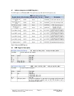
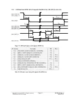
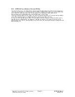
7.3.1
LBU Read from ERTEC 400 with separate Read/Write line (LBU_RDY_N active low)
LBU_CS_R_N/
LBU_CS_M_N
LBU_RD_N
LBU_A(20:0)A/
LBU_SEG(1:0)/
LBU_BE(1:0)_N
LBU_RDY_N
LBU_D(15:0)
t
CSRS
t
ARS
t
RRE
t
RDE
t
RTD
t
RDH
t
RAH
t
RCSH
t
RAP
t
RR
Figure 12: LBU-Read-Sequence with separate RD/WR line
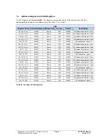
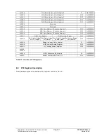
Parameter
Description
Min
Max
t
CSRS
chip select asserted to read pulse asserted delay
0 ns
t
ARS
address valid to read pulse asserted setup time
0 ns
t
RRE
read pulse asserted to ready enabled delay
5 ns
12 ns
t
RDE
read pulse asserted to data enable delay
5 ns
12 ns
t
RAP
ready active pulse width
17 ns
23 ns
t
RTD
ready asserted to data valid delay
5 ns
t
RCSH
read pulse deasserted to chip select deasserted delay
0 ns
t
RAH
address valid to read pulse deasserted hold time
0 ns
t
RDH
data valid/enabled to read pulse deasserted hold time
0 ns
12 ns
t
RR
read recovery time
25 ns
Table 22: LBU read access timing with seperate Read/Write line