Copyright © Siemens AG 2010. All rights reserved.
Page
57
ERTEC 400 Manual
Technical data subject to change
Version 1.2.2
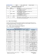
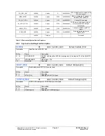
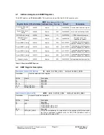
PCI_RES_ACK
0x0040
4 bytes
R
0x00000000
ACK for display of an implemented
SW reset request
MEM_SWAP
0x0044
4 bytes
R/W
0x00000000
Memory swapping in Segment 0
between ROM and RAM
PCI_INT_CTRL
0x0048
4 bytes
R/W
0x00000000
Control PCI interrupts
M_LOCK_CTRL
0x004C
4 bytes
R/W
0x00000000
AHB master lock enable. Master-
selective enable of AHB lock
functionality
ARM9_CTRL
0x0050
4 bytes
R/W
0x00001939
Controller of ARM9 and ETM
inputs
ARM9_WE
0x0054
4 bytes
R/W
0x00000000
Write protection register for
ARM9_CTRL
---------
0x0058
76 bytes
Reserved
Table 16: Overview of System Control Registers
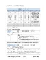
4.8.2
System Control Register Description
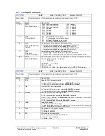
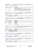
ID_REG
R
Addr.: 0x4000_2600
Default: 0x4026_0100
Description
Identification of ERTEC 400
Bit No.
Name
Description
31..16
ERTEC400-ID
ERTEC 400 identifier: 4026h (corresponds to the device ID of the AHB-PCI
bridge)
15..8
HW-RELEASE
HW release: 01h
7..0
Reserved
Reserved
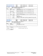
BOOT_REG
R
Addr.: 0x4000_2604 Default: Bootpins[2:0]
Description
Boot mode pins BOOT[2:0] can be read
Bit No.
Name
Description
31..3
----
Reserved
2 .. 0
BOOT[2:0]
Reading of BOOT[2.0] pin
CONFIG_REG
R
Addr.: 0x4000_2608
Default:Configpins[4:0]
Description
ERTEC 400 config pins CONFIG[4:0] can be read.
Bit No.
Name
Description
31..5
----
Reserved
4 .. 0
CONFIG[4:0]
Reading of CONFIG[4:0] pin

