Circuit descriptions and List of abbreviations
GB 97
VR120
9.
9.
Circuit descriptions and List of abbreviations
9.1
Switched-mode power supply PS (PS Part)
9.1.1
Technical data:
Mains voltage
: 195-264 Vrms
Maximum output
: 15W / 40W
(continuous /
maximum output)
Operating frequency
: 40 kHz
Efficiency
: approx. 75 % at
maximum output
Six different direct voltages are supplied on the power supply
outputs.
9.1.2
Functional principle:
This power supply functions in a similar way to a blocking
oscillator. In the supply voltage part [1300 to 2318], the mains
voltage is rectified and buffered in the capacitor [2318]. From
this direct voltage [2318] energy is transferred into the
transformer [5301, pins 1-3] during the conductive phase of
the switching transistor [7302] and is stored there as
magnetic energy. This energy is passed to the secondary
outputs on the power supply in the in the blocking phase of
the switching transistor [7302]. With the switch-on time of the
switching transistor [7302], the energy transferred in every
cycle is regulated in such a way that the output voltages
remain constant regardless of changes in the load or input
voltages. The power transistor is activated using the
integrated switch [7303] ( see figure 9-1 ).
9.1.3
Supply voltage part
The supply voltage part extends from the mains socket
[1300] to the capacitor [2318]. Using the diodes [6310, 6311,
6312 and 6313] the a.c. supply voltage is rectified and
buffered using the capacitor [2318]. The line reactor [5305]
and capacitor [2316] create a filter to keep interference
arising in the power supply away from the mains.
Components [1302], [3326] and [3323] protect the power
supply against short-term overvoltages in the mains, e.g.
caused by indirect effects from lightning.
9.1.4
Start-up with Mains-on:
Following connection to the mains, the capacitor [2310] is
loaded via the start-up resistor [3318] and a current source
between pin 8 and pin 6 on the IC [7303]. Once the voltage
on [2310] and therefore the supply voltage Vcc on the IC
[7303] has reached approx. 13V, the IC starts up and issues
pulses to its output on pin 5. These pulses are used to control
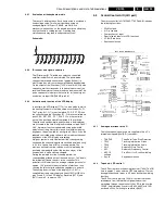
the gate on the power transistor [7302] ( see figure 9-2 ). The
frequency has a fixed setting in the IC (approx. 40 kHz). The
current input on the IC is approx. 5 mA in normal mode.
If Vcc drops to below approx. 10V (e.g. with power limitation)
or if Vcc exceeds around 15V (interruption of the control
loop), the output on the IC [7303, pin 5] is blocked. All output
voltages on the power supply, and therefore also Vcc,
decrease. Once Vcc has dropped to below approx. 6.5V, a
new start-up cycle begins. (See also “Overload, Power
Limitation, Burst Mode“ section)
Figure 9-1
200 µA
200 µA
200 µA
t
3
CTRL
1
DEMAG
5
DRIVER
GND
4
2
ISENSE
NC
7
6
VCC
8
VI
MC44608
start - up
management
C demag
65mV/45mV
Vcc
management
start - up
phase
switching phase
stand - by
stand - by
management
leading edge
blanking
PWM
comp
&
regulation
block
latch OFF phase
stand by
0
1
PWM
latch
thermal shutdown
&
buffer
output
OVP - out
quick OVP
UVL01
current and voltage
references
current mirror
current mirror
&
1
0
latched off phase
start up phase
&
1
0
&
7302
6307
2310
6305
3314
6304
3318
7300
+
5301
+
Содержание VR570
Страница 12: ...Direction for use GB 12 VR120 3 3 Direction for use RT111 RT116 RT112 RT114 RT123 RT121 RT128 ...
Страница 15: ...Direction for use GB 15 VR120 3 SAT VR870L VR870CC VR720 Set width 435 mm ...
Страница 56: ...Service modes Repair tips GB 56 VR120 5 Engineer s remarks ...
Страница 60: ...60 VR120 6 Block diagrams Waveforms 6 4 Supply voltages and Bus diagram 1941 SAT MOUSE o M63100BFP ...
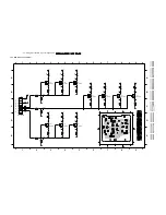
Страница 79: ...Circuit diagrams and PWB layouts Wiring diagram 79 VR120 7 7 16 Wiring Diagram Motherboard ...
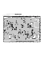
Страница 80: ...80 VR120 7 Circuit diagrams and PWB layouts Wiring diagram 7 17 Mother board solder side 7172 CLOCK ADJUST ...
Страница 81: ...Circuit diagrams and PWB layouts Wiring diagram 81 VR120 7 Engineer s remarks ...
Страница 82: ...82 VR120 7 Circuit diagrams and PWB layouts Wiring diagram Engineer s remarks ...
Страница 83: ...Circuit diagrams and PWB layouts Wiring diagram 83 VR120 7 7 18 Mother board component side ...
Страница 119: ...Tape deck GB 119 VR120 10 ...
Страница 123: ...Tape deck GB 123 VR120 10 Engineer s remarks ...

