Dismantling instructions
GB 48
VR120
4.
4.3
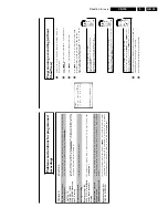
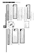
Dismantling the drive (Figure 4-3, 4-5 and 4-6)
Preparation
Remove the housing cover as described in section 1.
Remove the front panel as described in section 3.
–
Undo the two screws (B) of the stay and pull it up to
remove it.
–
Push back lift by 5 cm after releasing both lift stops.
–
Undo and remove the four fastening screws (C) of the
drive.
–
Undo and remove the ground screw (D) at the rear.
–
(For this purpose, insert the screwdriver through the hole
in the back panel).
–
Remove the cables from the drive.
–
Bend back the guard of the scanner cable.
–
Remove the scanner cable from the socket.
–
Return the lift into the ”Eject” position.
–
Slightly lift the left rear side of the drive to undo the
connector to the capstan motor.
–
Press both catches (S) together with fine pliers and lift
the drive around the snapholders.
–
The drive may be separated from the motherboard.
Assembly
Assemble in reverse order.
Important
Observe that the cables (K1; K2; K3) are positioned in the
supports on the rear of the frame and that the ground screw
(D) is screwed in!
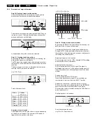
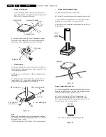
Figure 4-5
Figure 4-6
S
S
C
C
D
C
C
S
C
C
D
C
C
S
D
Service position
Содержание VR570
Страница 12: ...Direction for use GB 12 VR120 3 3 Direction for use RT111 RT116 RT112 RT114 RT123 RT121 RT128 ...
Страница 15: ...Direction for use GB 15 VR120 3 SAT VR870L VR870CC VR720 Set width 435 mm ...
Страница 56: ...Service modes Repair tips GB 56 VR120 5 Engineer s remarks ...
Страница 60: ...60 VR120 6 Block diagrams Waveforms 6 4 Supply voltages and Bus diagram 1941 SAT MOUSE o M63100BFP ...
Страница 79: ...Circuit diagrams and PWB layouts Wiring diagram 79 VR120 7 7 16 Wiring Diagram Motherboard ...
Страница 80: ...80 VR120 7 Circuit diagrams and PWB layouts Wiring diagram 7 17 Mother board solder side 7172 CLOCK ADJUST ...
Страница 81: ...Circuit diagrams and PWB layouts Wiring diagram 81 VR120 7 Engineer s remarks ...
Страница 82: ...82 VR120 7 Circuit diagrams and PWB layouts Wiring diagram Engineer s remarks ...
Страница 83: ...Circuit diagrams and PWB layouts Wiring diagram 83 VR120 7 7 18 Mother board component side ...
Страница 119: ...Tape deck GB 119 VR120 10 ...
Страница 123: ...Tape deck GB 123 VR120 10 Engineer s remarks ...


