enabling
innovative
electronics
Ossila Ltd
Copyright © 2009-2015
62
“The table details the time required to within reach 0.1% of final value after source level command is
processed on a fixed range” (Keithley 2612B datasheet).
Organic transistors have much longer transient time. Accordingly, IEEE
19
standard for OFET
characterisation recommends a minimum settling time (dwell time) of 10 ms up to 100 ms for each
data point. The appropriate settling time depends on the dielectric, organic semiconductor, OFET
architecture and measurement settings.
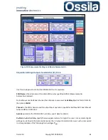
For accurate measurements, indicative Delay values are 100/200 ms for each gate sweeps (GATE
Delay, with
V) and 10 to 20 ms for each drain current acquired (DRAIN Delay, with
). These values refer to OFF
ON sweep. For ON
OFF sweep, the required delay times
are higher. Refer to the
Measurement and Accuracy
section for more detailed information on
Settling Time.
Important:
For IV Sweeps, SuperFACT will always force the SMU GATE to wait at least 5 ms after
V
GS
,
i
is applied.
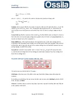
Current Limit
specifies the maximum gate current range (
I
GS
) that the GATE source is allowed to
induce across the target (OFET, for example). If the current exceed
Current Limit
, the SMU will
complete the acquisition without increasing the voltage further to avoid damaging the internal
circuitry. Refer to the
Measurement and Accuracy
section for the appropriate setting of
Current
Limit
and its relation with measurement accuracy.
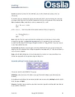
Max Gate Current
is a User’s selected threshold on I
GS
as leakage current. More specifically, Max
Gate Current is the maximum I
GS
(V
DS
) that the User deems acceptable for the DUT. If I
leak
> I
GS
,
SuperFACT stops acquiring the I-V curves for the particular
V
GS
for which the limit has been exceeded
and moves to acquire the next (if any) DUT.
Tip:
Use
Max Gate Current
to speed up data acquisition by avoiding measuring transistors which
present very high gate current leakage.
Note:
Set Max Gate Current to be lower than
Current Limit
. IEEE recommends gate current leakage
to be less than 1% of the drain current I
DS
(V
DS
).
Max Gate Current
is disabled if its value matches
Current Limit
.
19
IEEE Standard for Test Methods for the Characterization of Organic Transistors and Materials; IEEE
Std
1620-2008.

