enabling
innovative
electronics
Ossila Ltd
Copyright © 2009-2015
39
Note:
Since the derivative of a function
y
=
f(x)
at a point
y
0
is the slope of the tangent curve of
f(x)
at
y
0
,
the derivative of straight line
y
s
=
αx
gives the same numerical value (α) for any point
y
0
belonging
to
y
s
. In other words, the slope of the linear fit of a straight line y=
f(x)
and the derivative at any of its
points y
0
are the same. Therefore for a straight line, Eqs. 9 and 10 reduce to Eqs. 4 and 8. Most
importantly, to the extent the drain current is weakly dependent on V
GS
, Eqs. 4 and 8 can be
considered to be a sufficiently good approximation of Eqs. 10 and 11.
These considerations are particularly important in the field of organic electronic because, with few
notable exceptions, OFET/TFT mobilities are gate-voltage dependent. However, for weakly
dependence, Eqs. 4 and 8 and Eqs. 9 and 10 yield approximately the same numerical value for the
field effect mobility.
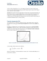
Transfer characteristic curves: ideal and real behaviour
For an ideal TC curves the drain current is zero for V
GS
<V
T
and increases rapidly for V
GS
>V
T
. In actual
fact, the relation between drain current and both gate and drain voltage is more involved
11
. For the
sake of simplicity, we neglect the details of the functional dependence of I
DS
on the driving voltages,
and simply assume that for a
well-behaved
FET, the current for V
GS
< V
Th
is very small when
compared with I
DS
for V
GS
>> V
T
.
Notwithstanding these simplifications, depending on the value of V
GS
, a transistor can be found in
two different operation regions:
Subthreshold
or
Cutoff
(for V
GS
< V
Th
) and
ON
(for V
GS
> V
Th
). It
follows that a FET can be considered as two-state device (bit) with the state
OFF
(logical state 0) and
ON
(logical state 1) corresponding to the two operation regions Cutoff and ON respectively.
A good transistor must therefore output a tiny (ideally zero) current while OFF and switch on very
steeply as V
GS
approaches V
Th,
see Eq. 16, so to allow for fast (steep) ON/OFF transition.
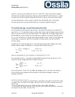
Since I
Th
is the largest current that a transistor output before entering the ON region, for
characterisation purpose, it is useful to consider the threshold current to be the OFF current of the
FET. We therefore define the OFF current as
I
OFF
= I
Th
= I
DS
(V
Th
).
Eq. 11
Similarly, the ON current I
ON
is defined as
I
ON
= I
DS
(V
ON
),
Eq. 12
where V
ON
is the typical operational gate voltage applied to the transistor to switch it ON. V
ON
is
therefore a not well-defined quantity, and its actual numerical value can depend on the
application/purpose of the transistor itself. For example, for inorganic FETs complying with TTL
11
Refer to references 6, 7 and 8
for more detailed analysis of the mathematical relationship between I
DS
,
applied voltages and FET intrinsic material properties.

