enabling
innovative
electronics
Ossila Ltd
Copyright © 2009-2015
77
Mobility algorithms: interval of validity, issues and caveats
The field-effect transistor figures of merit are calculated under the assumption that the transistor
model detailed in the
Transfer Characteristics
section applies to the DUT. For the sake of this
manual, we call a device that complies with such a model
well behaved
.
Figures of merit calculated
from devices that categorically fails to satisfy the standard field effect model should not be
considered valid.
SuperFACT automatically runs a basic check for the validity of the transistor models when it executes
the mobility computation algorithm; however, a visual inspection of the I-V and TC curves by the
user is still required to avoid taking into account data extrapolated from DUT non complying with the
field effect transistor model.
Interval of validity
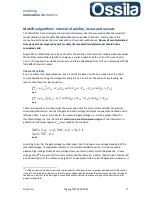
Eqs. 4 and 8 (or their generalisations, Eqs. 9 and 10) are based on the assumption that the drain
current depends on the gate voltage according to Eqs. 1 and 2. For the sake of easy reading, we
rewrite here these last two equations
with
Eq. 3
with
Eq. 6
These two equations are valid under the assumption that the drain current satisfies the gradual
channel approximation, and that the gate and drain voltage satisfy the inequality as detailed on the
left side of Eqs. 3 and 6. In particular, the measured gate voltage V
GS,i
must be greater than the
threshold voltage (i.e. Eqs. 3 and 8 are valid only in the
ON
operation region of the transistor). In
addition for the linear regime, V
GS,i
must satisfies the condition
=
>>
Eq. 30
According to Eq. 30, the gate voltage must be larger than the drain source voltage deducted of the
threshold voltage. To complicate matters, for non-optimised R&D devices, it is not unusual to
observe high-voltage stress. Severe voltage stress can result in drain current degradation. In case
voltage stress
24
is present, the transistor model, and therefore Eq. 3 and 6, should not be considered
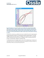
a valid description of the system; see Fig 16 for an example of drain current degradation. However, if
24
Voltage stress can be due to intrinsic semiconductor deficiency (traps, impurity) architectural of fabrication
issue etc, or simply be an indication that the gate voltage applied exceeds the maximum operation voltage of
the device. Clearly at the R&D stage it may not be known yet the operational range of the new material or
device architecture.

