


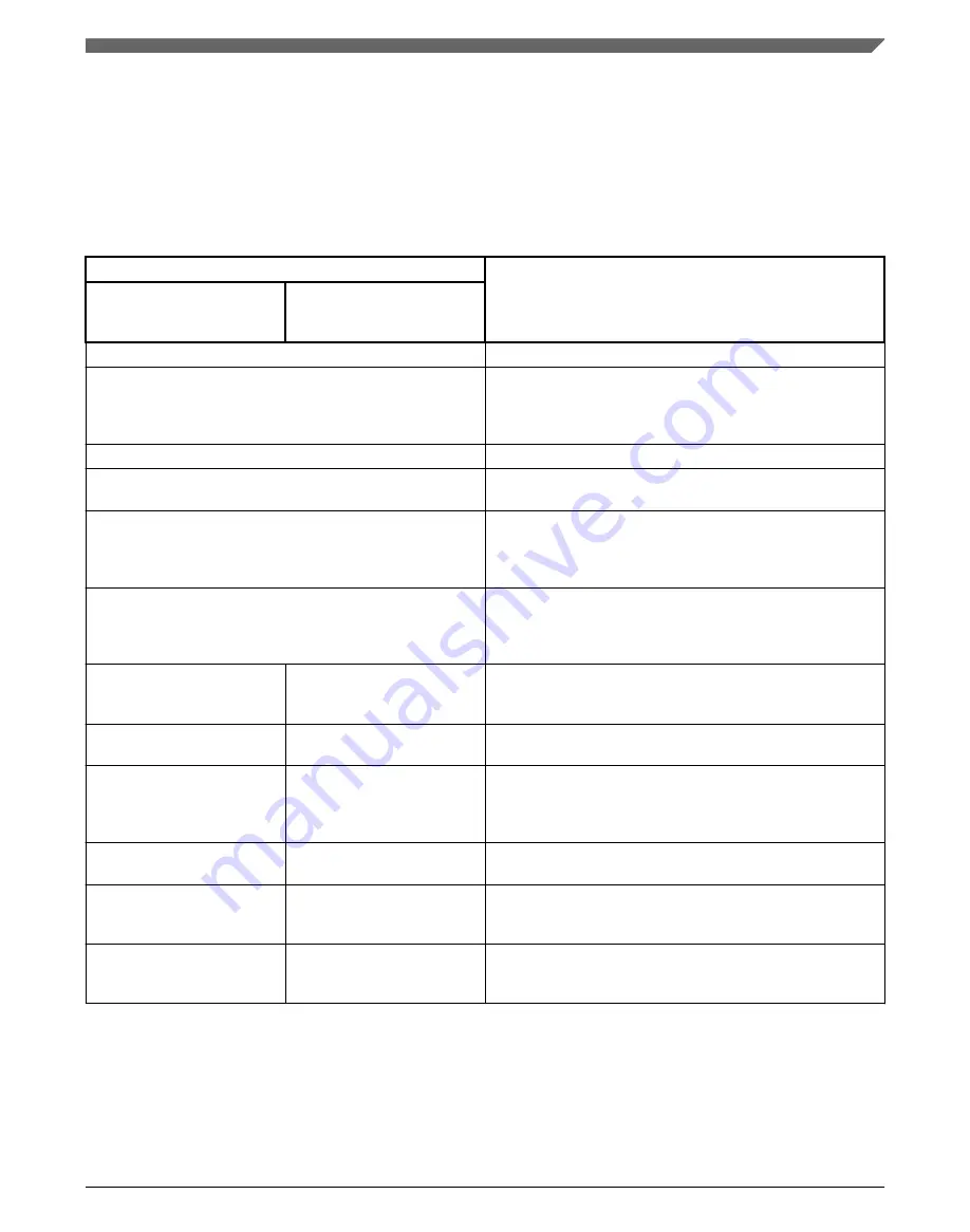
The eDMA design supports the following hardware service request sequence. Note that
the exact timing from Cycle 7 is a function of the response times for the channel's read
and write accesses. In the case of an internal peripheral bus read and internal SRAM
write, the combined data phase time is 4 cycles. For an SRAM read and internal
peripheral bus write, it is 5 cycles.
Table 20-5. Hardware service request process
Cycle
Description
With internal peripheral
bus read and internal
SRAM write
With SRAM read and
internal peripheral bus
write
1
eDMA peripheral request is asserted.
2
The eDMA peripheral request is registered locally in the
eDMA module and qualified. TCD
n
_CSR[START] bit initiated
requests start at this point with the registering of the user
write to TCD
n
word 7.
3
Channel arbitration begins.
4
Channel arbitration completes. The transfer control descriptor
local memory read is initiated.
5–6
The first two parts of the activated channel's TCD is read from
the local memory. The memory width to the eDMA engine is
64 bits, so the entire descriptor can be accessed in four
cycles
7
The first system bus read cycle is initiated, as the third part of
the channel's TCD is read from the local memory. Depending
on the state of the crossbar switch, arbitration at the system
bus may insert an additional cycle of delay here.
8–11
8–12
The last part of the TCD is read in. This cycle represents the
first data phase for the read, and the address phase for the
destination write.
12
13
This cycle represents the data phase of the last destination
write.
13
14
The eDMA engine completes the execution of the inner minor
loop and prepares to write back the required TCD
n
fields into
the local memory. The TCD
n
word 7 is read and checked for
channel linking or scatter/gather requests.
14
15
The appropriate fields in the first part of the TCD
n
are written
back into the local memory.
15
16
The fields in the second part of the TCD
n
are written back into
the local memory. This cycle coincides with the next channel
arbitration cycle start.
16
17
The next channel to be activated performs the read of the first
part of its TCD from the local memory. This is equivalent to
Cycle 4 for the first channel's service request.
Assuming zero wait states on the system bus, DMA requests can be processed every 9
cycles. Assuming an average of the access times associated with internal peripheral bus-
to-SRAM (4 cycles) and SRAM-to-internal peripheral bus (5 cycles), DMA requests can
Chapter 20 Enhanced Direct Memory Access (eDMA)
K32 L2A Reference Manual, Rev. 2, 01/2020
NXP Semiconductors
463
Содержание K32 L2A Series
Страница 2: ...K32 L2A Reference Manual Rev 2 01 2020 2 NXP Semiconductors...
Страница 42: ...K32 L2A Reference Manual Rev 2 01 2020 42 NXP Semiconductors...
Страница 122: ...Flash Memory Clock K32 L2A Reference Manual Rev 2 01 2020 122 NXP Semiconductors...
Страница 146: ...Module operation in low power modes K32 L2A Reference Manual Rev 2 01 2020 146 NXP Semiconductors...
Страница 158: ...Debug and security K32 L2A Reference Manual Rev 2 01 2020 158 NXP Semiconductors...
Страница 174: ...Module Signal Description Tables K32 L2A Reference Manual Rev 2 01 2020 174 NXP Semiconductors...
Страница 246: ...Application information K32 L2A Reference Manual Rev 2 01 2020 246 NXP Semiconductors...
Страница 322: ...Kinetis Bootloader Status Error Codes K32 L2A Reference Manual Rev 2 01 2020 322 NXP Semiconductors...
Страница 344: ...Application initialization information K32 L2A Reference Manual Rev 2 01 2020 344 NXP Semiconductors...
Страница 374: ...CMP Trigger Mode K32 L2A Reference Manual Rev 2 01 2020 374 NXP Semiconductors...
Страница 384: ...Functional description K32 L2A Reference Manual Rev 2 01 2020 384 NXP Semiconductors...
Страница 592: ...Application Information K32 L2A Reference Manual Rev 2 01 2020 592 NXP Semiconductors...
Страница 602: ...Initialization and application information K32 L2A Reference Manual Rev 2 01 2020 602 NXP Semiconductors...
Страница 656: ...Functional Description K32 L2A Reference Manual Rev 2 01 2020 656 NXP Semiconductors...
Страница 664: ...Functional Description K32 L2A Reference Manual Rev 2 01 2020 664 NXP Semiconductors...
Страница 744: ...Functional description K32 L2A Reference Manual Rev 2 01 2020 744 NXP Semiconductors...
Страница 762: ...Functional description K32 L2A Reference Manual Rev 2 01 2020 762 NXP Semiconductors...
Страница 806: ...Functional description K32 L2A Reference Manual Rev 2 01 2020 806 NXP Semiconductors...
Страница 868: ...Integer square root K32 L2A Reference Manual Rev 2 01 2020 868 NXP Semiconductors...
Страница 976: ...Functional description K32 L2A Reference Manual Rev 2 01 2020 976 NXP Semiconductors...
Страница 1012: ...Functional description K32 L2A Reference Manual Rev 2 01 2020 1012 NXP Semiconductors...
Страница 1094: ...Functional description K32 L2A Reference Manual Rev 2 01 2020 1094 NXP Semiconductors...
Страница 1132: ...Functional description K32 L2A Reference Manual Rev 2 01 2020 1132 NXP Semiconductors...
Страница 1182: ...Functional description K32 L2A Reference Manual Rev 2 01 2020 1182 NXP Semiconductors...
Страница 1290: ...Functional description K32 L2A Reference Manual Rev 2 01 2020 1290 NXP Semiconductors...
Страница 1344: ...USB Voltage Regulator Module Signal Descriptions K32 L2A Reference Manual Rev 2 01 2020 1344 NXP Semiconductors...
Страница 1356: ...Initialization Application Information K32 L2A Reference Manual Rev 2 01 2020 1356 NXP Semiconductors...