


Memory
MCF51CN128 Reference Manual, Rev. 6
4-32
Freescale Semiconductor
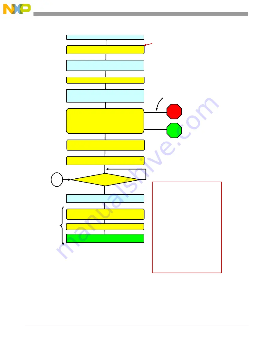
N = number of cycles for SIM to release
internal reset. Adder of 16 imposed by the
ColdFire core.
BKGD=0 during reset will
ensure that ENBDM comes up "1"
secure state unknown / unpowered
secure state unknown, CPU halted, FEI 10MHz
clock, sync required
secure state unknown,, CPU halted, FEI 10MHz
clock, synchronized to debugger
hold BKGD=0, apply power, wait N+16 cycles for
POR to de-assert
SYNC
set PRDIV8 and clock divider fields in CSR3
write xcsr[31:24]=0x87 to initiate erase/verify
of flash memory
read xcsr[25] to confirm
erase/verify complete
on-chip flash is erased and un-secure
write csr2[25:24]=11 to initiate BDM reset to halt or
write csr2[25:0]=01 to initiate BDM reset to run
Device is unsecure
no
yes
xcsr[31:24]==0x87
STOP
STOP
already unsecured
error condition
check code or device
The FTSR is responsible for supplying
an "erase completed and verified" flag
for use by the core in this step.
FLL Enabled, Internal Reference (FEI)
at 10MHz is reset default for the ICS
Ways to enter BDM halt mode:
1. BKGD=0 during POR
2. BKGD=0 during BDM reset
3. BFHBR=1 during BDM reset
4. COP reset and CSR2[COPHR]=1
5. Illegal op code reset and
CSR2[IOPHR]=1
6. Illegal address reset and
CSR2[IADHR]=1
7. Loss of Lock reset with
CSR2[LOLHR]=1
8. Issue BACKGROUND cmd via BDM
interface
9. HALT instruction
10.BDM breakpoint
11.ColdFire Fault-on-Fault
Of these, only method (1) is
guaranteed to work under all
circumstances.
Read XCSR
xcsr[31:24] != 1000 01-1
xcsr[25]=0
Delay "TBD" cycles
A
The write IS required
.
1
1. The last three steps are optional, but
recommended.


