Appendix D – GTXI Buffer Board
159
define the first address of the user-defined memory block
MEMS0. The address can be calculated by multiplying
the value in bits 0-7 by 64KB. The default value for these
bits is all ‘0’s.
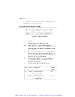
Memory Mask Register (MMR)
Internal address (IA) is 4.
Bit# 15-7
6 5-0
F
UNCTION
U
BEM
MSE5-0
Table D-8: Memory Register MMR Bit Functions
U
Unused
BEM
Buffer Enable Mode. ‘0’ – always (default), ‘1’ –
effective. In the ‘always’ mode the ISA signals are
always enabled through the GTXI buffer. In the effective
mode, those signals are enabled only when a GTXI
assigned resource is accessed. In this mode the noise
generated by the GTXI is reduced.
MSE
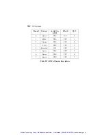
Memory Block Enable. ‘0’ – block disabled. ‘1’ – block
enabled. See the table below for bit assignments. The
default value of these bits is 0 (all disabled). The last
block is user-defined, and is defined by writing the first
address of the block to MSA register and the last address
of the block to the MEA register. In both cases, the
resolution is 64Kbyte
Artisan Technology Group - Quality Instrumentation ... Guaranteed | (888) 88-SOURCE | www.artisantg.com
Содержание Geotest GT7700
Страница 113: ...98 GTXI User s Guide Artisan Technology Group Quality Instrumentation Guaranteed 888 88 SOURCE www artisantg com ...
Страница 139: ...Artisan Technology Group Quality Instrumentation Guaranteed 888 88 SOURCE www artisantg com ...
Страница 145: ...Artisan Technology Group Quality Instrumentation Guaranteed 888 88 SOURCE www artisantg com ...
Страница 191: ...176 GTXI User s Guide Artisan Technology Group Quality Instrumentation Guaranteed 888 88 SOURCE www artisantg com ...
Страница 209: ...Chapter 3 Index 194 Artisan Technology Group Quality Instrumentation Guaranteed 888 88 SOURCE www artisantg com ...

