287
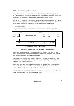
SCI3 operates as follows when transmitting data.
SCI3 monitors bit TDRE in SSR, and when it is cleared to 0, recognizes that data has been written
to TDR and transfers data from TDR to TSR. It then sets bit TDRE to 1 and starts transmitting. If
bit TIE in SCR3 is set to 1 at this time, a TXI request is made.
When clock output mode is selected, SCI3 outputs 8 serial clock pulses. When an external clock
is selected, data is output in synchronization with the input clock.
Serial data is transmitted from the TXD3x pin in order from the LSB (bit 0) to the MSB (bit 7).
When the MSB (bit 7) is sent, checks bit TDRE. If bit TDRE is cleared to 0, SCI3 transfers data
from TDR to TSR, and starts transmission of the next frame. If bit TDRE is set to 1, SCI3 sets bit
TEND to 1 in SSR, and after sending the MSB (bit 7), retains the MSB state. If bit TEIE in SCR3
is set to 1 at this time, a TEI request is made.
After transmission ends, the SCK pin is fixed at the high level.
Note:
Transmission is not possible if an error flag (OER, FER, or PER) that indicates the data
reception status is set to 1. Check that these error flags are all cleared to 0 before a
transmit operation.
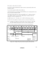
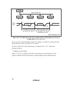
Figure 10.12 shows an example of the operation when transmitting in synchronous mode.
Serial
clock
Serial
data
Bit 1
Bit 0
Bit 7
Bit 0
1 frame
1 frame
Bit 1
Bit 6
Bit 7
TDRE
TEND
LSI
operation
User
processing
TXI request
Data written
to TDR
TDRE cleared
to 0
TXI request
TEI request
Figure 10.12 Example of Operation when Transmitting in Synchronous Mode


