12
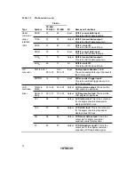
Table 1.2
Pin Functions (cont)
Pin No.
Type
Symbol
FP-80A
TFP-80C
FP-80B
I/O
Name and Functions
Serial
communi-
RXD
31
22
24
Input
SCI3-1 receive data input:
This is the SCI31 data input pin.
cation
interface
TXD
31
23
25
Output SCI3-1 transmit data output:
This is the SCI31 data output pin.
(SCI)
SCK
31
21
23
I/O
SCI3-1 clock I/O:
This is the SCI31 clock I/O pin.
RXD
32
70
72
Input
SCI3-2 receive data input:
This is the SCI32 data input pin.
TXD
32
71
73
Output SCI3-2 transmit data output:
This is the SCI32 data output pin.
SCK
32
69
71
I/O
SCI3-2 clock I/O:
This is the SCI32 clock I/O pin.
A/D
converter
AN7 to An0 1
80 to 74
3 to 1
80 to 76
Input
Analog input channels 7 to 0:
These are analog data input channels to
the A/D converter
ADTRG
14
16
Input
A/D converter trigger input:
This is the external trigger input pin to
the A/D converter
LCD
controller/
COM
4
to
COM
1
33 to 36
35 to 38
Output LCD common output: These are the
LCD common output pins.
driver
SEG
32
to
SEG
1
68 to 37
70 to 39
Output LCD segment output: These are the
LCD segment output pins.
CL1
68
70
Output LCD latch clock: This is the output pin
for the segment external expansion
display data latch clock.
CL2
67
69
Output LCD shift clock: This is the output pin
for the segment external expansion
display data shift clock.
DO
66
68
Output LCD serial data output: This is the
output pin for segment external
expansion serial display data.
M
65
67
Output LCD alternation signal: This is the
output pin for the segment external
expansion LCD alternation signal.

