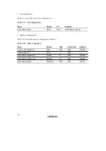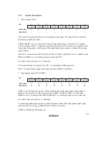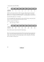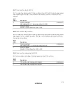
218
9.5.3
Noise Canceler
The noise canceler consists of a digital low-pass filter that eliminates high-frequency component
noise from the pulses input from the input capture input pin. The noise canceler is set by NCS* in
PMR3.
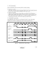
Figure 9.8 shows a block diagram of the noise canceler.
C
D
Q
Latch
C
D
Q
Latch
C
D
Q
Latch
C
D
Q
Latch
C
D
Q
Latch
Match
detector
Noise
canceler
output
Sampling
clock
Input capture
input signal
Sampling clock
∆
t
∆
t: Set by CKS1 and CKS0
Figure 9.8 Noise Canceler Block Diagram
The noise canceler consists of five latch circuits connected in series and a match detector circuit.
When the noise cancellation function is not used (NCS = 0), the system clock is selected as the
sampling clock When the noise cancellation function is used (NCS = 1), the sampling clock is the
internal clock selected by CKS1 and CKS0 in TMG, the input capture input is sampled on the
rising edge of this clock, and the data is judged to be correct when all the latch outputs match. If
all the outputs do not match, the previous value is retained. After a reset, the noise canceler output
is initialized when the falling edge of the input capture input signal has been sampled five times.
Therefore, after making a setting for use of the noise cancellation function, a pulse with at least
five times the width of the sampling clock is a dependable input capture signal. Even if noise
cancellation is not used, an input capture input signal pulse width of at least 2ø or 2ø
SUB
is
necessary to ensure that input capture operations are performed properly
Note: * An input capture signal may be generated when the NCS bit is modified.

