background image

243

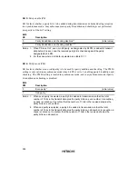
3.   Event counter L (ECL)

ECL is an 8-bit read-only up-counter that operates either as an independent 8-bit event counter or
as the lower 8-bit up-counter of a 16-bit event counter configured in combination with ECH.  The
event clock from the external asynchronous event AEVL pin is used as the input clock source.
ECL can be cleared to H'00 by software, and is also initialized to H'00 upon reset.

ECL7

ECL2

ECL1

ECL0

ECL6

ECL5

ECL4

ECL3

7

6

5

4

3

2

1

0

0

0

0

0

0

0

0

0

R

R

R

R

R

R

R

R

Bit

Initial Value

Read/Write

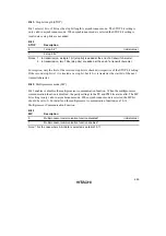
4.   Clock stop register 2 (CKSTPR2)

WDCKSTP PWCKSTP LDCKSTP

AECKSTP

7

6

5

4

3

2

1

0

1

1

1

1

1

1

1

1

R/W

R/W

R/W

R/W

Bit

Initial value

Read/Write

CKSTPR2 is an 8-bit read/write register that performs module standby mode control for peripheral
modules.  Only the bit relating to the asynchronous event counter is described here.  For details of
the other bits, see the sections on the relevant modules.

Bit 3: Asynchronous event counter module standby mode control (AECKSTP)

Bit 3 controls setting and clearing of module standby mode for the asynchronous event counter.

AECKSTP

Description

0

Asynchronous event counter is set to module standby mode

1

Asynchronous event counter module standby mode is cleared

(initial value)

Содержание H8/3822R

Страница 1: ...H8 3827R Series H8 3827R HD6473827R HD6433827R H8 3826R HD6433826R H8 3825R HD6433825R H8 3824R HD6433824R H8 3823R HD6433823R H8 3822R HD6433822R Hardware Manual ADE 602 196 Rev 1 0 9 15 99 Hitachi Ltd ...

Страница 2: ...of bodily injury such as aerospace aeronautics nuclear power combustion control transportation traffic safety equipment or medical equipment for life support 4 Design your application so that the product is used within the ranges guaranteed by Hitachi particularly for maximum rating operating supply voltage range heat radiation characteristics installation conditions and other characteristics Hita...

Страница 3: ... a system on a chip architecture that includes such peripheral functions as a as an LCD controller driver six timers a 14 bit PWM a two channel serial communication interface and an A D converter This allows H8 3827R Series devices to be used as embedded microcomputers in systems requiring LCD display This manual describes the hardware of the H8 3827R Series For details on the instruction set refe...

Страница 4: ... 3 2 Memory Data Formats 19 2 4 Addressing Modes 20 2 4 1 Addressing Modes 20 2 4 2 Effective Address Calculation 22 2 5 Instruction Set 26 2 5 1 Data Transfer Instructions 28 2 5 2 Arithmetic Operations 30 2 5 3 Logic Operations 31 2 5 4 Shift Operations 31 2 5 5 Bit Manipulations 33 2 5 6 Branching Instructions 37 2 5 7 System Control Instructions 39 2 5 8 Block Data Transfer Instruction 40 2 6 ...

Страница 5: ...t Operations 78 3 3 6 Interrupt Response Time 83 3 4 Application Notes 84 3 4 1 Notes on Stack Area Use 84 3 4 2 Notes on Rewriting Port Mode Registers 85 Section 4 Clock Pulse Generators 87 4 1 Overview 87 4 1 1 Block Diagram 87 4 1 2 System Clock and Subclock 87 4 2 System Clock Generator 88 4 3 Subclock Generator 91 4 4 Prescalers 93 4 5 Note on Oscillators 94 Section 5 Power Down Modes 95 5 1 ...

Страница 6: ... Mode 110 5 7 Active Medium Speed Mode 111 5 7 1 Transition to Active Medium Speed Mode 111 5 7 2 Clearing Active Medium Speed Mode 111 5 7 3 Operating Frequency in Active Medium Speed Mode 111 5 8 Direct Transfer 112 5 8 1 Overview of Direct Transfer 112 5 8 2 Direct Transition Times 113 5 8 3 Notes on External Input Signal Changes before after Direct Transition 115 5 9 Module Standby Mode 116 5 ...

Страница 7: ...scription 150 8 4 3 Pin Functions 151 8 4 4 Pin States 152 8 5 Port 5 153 8 5 1 Overview 153 8 5 2 Register Configuration and Description 153 8 5 3 Pin Functions 156 8 5 4 Pin States 156 8 5 5 MOS Input Pull Up 157 8 6 Port 6 157 8 6 1 Overview 157 8 6 2 Register Configuration and Description 158 8 6 3 Pin Functions 159 8 6 4 Pin States 159 8 6 5 MOS Input Pull Up 160 8 7 Port 7 160 8 7 1 Overview...

Страница 8: ... 2 Register Descriptions 178 9 2 3 Timer Operation 182 9 2 4 Timer A Operation States 183 9 3 Timer C 184 9 3 1 Overview 184 9 3 2 Register Descriptions 186 9 3 3 Timer Operation 190 9 3 4 Timer C Operation States 192 9 4 Timer F 193 9 4 1 Overview 193 9 4 2 Register Descriptions 196 9 4 3 CPU Interface 203 9 4 4 Operation 206 9 4 5 Application Notes 209 9 5 Timer G 210 9 5 1 Overview 210 9 5 2 Re...

Страница 9: ... Serial mode register SMR 253 10 2 6 Serial control register 3 SCR3 256 10 2 7 Serial status register SSR 260 10 2 8 Bit rate register BRR 264 10 2 9 Clock stop register 1 CKSTPR1 268 10 2 10 Serial Port Control Register SPCR 269 10 3 Operation 271 10 3 1 Overview 271 10 3 2 Operation in Asynchronous Mode 275 10 3 3 Operation in Synchronous Mode 284 10 3 4 Multiprocessor Communication Function 291...

Страница 10: ...on Modes 319 12 4 Interrupts 319 12 5 Typical Use 319 12 6 Application Notes 322 Section 13 LCD Controller Driver 323 13 1 Overview 323 13 1 1 Features 323 13 1 2 Block Diagram 324 13 1 3 Pin Configuration 325 13 1 4 Register Configuration 325 13 2 Register Descriptions 326 13 2 1 LCD Port Control Register LPCR 326 13 2 2 LCD Control Register LCR 328 13 2 3 LCD Control Register 2 LCR2 330 13 2 4 C...

Страница 11: ...Timing 372 15 4 Output Load Circuit 376 15 5 Resonator Equivalent Circuit 376 Appendix A CPU Instruction Set 377 A 1 Instructions 377 A 2 Operation Code Map 385 A 3 Number of Execution States 387 Appendix B Internal I O Registers 393 B 1 Addresses 393 B 2 Functions 397 Appendix C I O Port Block Diagrams 448 C 1 Block Diagrams of Port 1 448 C 2 Block Diagrams of Port 3 451 C 3 Block Diagrams of Por...

Страница 12: ... Together these functions make the H8 3827R Series ideally suited for embedded applications in systems requiring low power consumption and LCD display Models in the H8 3827R Series are the H8 3822R with on chip 16 kbyte ROM and 1 kbyte RAM the H8 3823R with 24 kbyte ROM and 1 kbyte RAM the H8 3824R with 32 kbyte ROM and 2 kbyte RAM the H8 3825R with 40 kbyte ROM and 2 kbyte RAM the H8 3826R with 4...

Страница 13: ...operations between registers MOV instruction for data transfer between memory and registers Typical instructions Multiply 8 bits 8 bits Divide 16 bits 8 bits Bit accumulator Register indirect designation of bit position Interrupts 36 interrupt sources 13 external interrupt sources IRQ4 to IRQ0 WKP7 to WKP0 23 internal interrupt sources Clock pulse generators Two on chip clock pulse generators Syst...

Страница 14: ...it timer Count up timer able to count asynchronous external events independently of the MCU s internal clocks Timer C 8 bit timer Count up down timer with selection of seven internal clock signals or event input from external pin Auto reloading Timer F 16 bit timer Can be used as two independent 8 bit timers Count up timer with selection of four internal clock signals or event input from external ...

Страница 15: ...cation function 14 bit PWM Pulse division PWM output for reduced ripple Can be used as a 14 bit D A converter by connecting to an external low pass filter A D converter Successive approximations using a resistance ladder 8 channel analog input pins Conversion time 31 ø or 62 ø per channel LCD controller driver LCD controller driver equipped with a maximum of 32 segment pins and four common pins Ch...

Страница 16: ...23RW 80 pin TQFP TFP 80C HD6433824RH 80 pin QFP FP 80A ROM 32 kbytes HD6433824RF 80 pin QFP FP 80B RAM 2 kbytes HD6433824RW 80 pin TQFP TFP 80C HD6433825RH 80 pin QFP FP 80A ROM 40 kbytes HD6433825RF 80 pin QFP FP 80B RAM 2 kbytes HD6433825RW 80 pin TQFP TFP 80C HD6433826RH 80 pin QFP FP 80A ROM 48 kbytes HD6433826RF 80 pin QFP FP 80B RAM 2 kbytes HD6433826RW 80 pin TQFP TFP 80C HD6433827RH HD6473...

Страница 17: ...b Clock OSC V SS V SS V CC CV CC RES TEST H8 300L CPU LCD Power Supply ROM 60k 48k 40k 32k 24k 16k RAM 2k 1k Timer A Timer C Timer F Timer G Asynchronous counter Serial communication interface 3 1 Serial communication interface 3 2 14 bit PWM WDT LCD Controller A D 10bit V0 V1 V2 V3 PA3 COM4 PA2 COM3 PA1 COM2 PA0 COM1 P87 SEG32 CL1 P86 SEG31 CL2 P85 SEG30 DO P84 SEG29 M P83 SEG28 P82 SEG27 P81 SEG...

Страница 18: ...IRQ0 AVCC PB0 AN0 PB1 AN1 PB2 AN2 PB3 AN3 PB4 AN4 PB5 AN5 PB6 AN6 PB 7 AN 7 AV SS X 1 X 2 V SS OSC 2 OSC 1 TEST RES P1 0 TMOW P1 1 TMOFL P1 2 TMOFH P1 3 TMIG P1 4 IRQ 4 ADTRG P1 5 IRQ 1 TMIC P1 6 IRQ 2 P1 7 IRQ 3 TMIF P3 0 PWM P3 1 UD P3 2 RESO P53 WKP3 SEG4 P52 WKP2 SEG3 P51 WKP1 SEG2 P50 WKP0 SEG1 PA0 COM1 PA1 COM2 PA2 COM3 PA3 COM4 VCC V0 V1 V2 V3 VSS CVCC P37 AEVL P36 AEVH P35 TXD31 P34 RXD31 ...

Страница 19: ...P 7 SEG8 P5 6 WKP 6 SEG7 P5 5 WKP 5 SEG6 P5 4 WKP 4 SEG5 P5 3 WKP 3 SEG4 P5 2 WKP 2 SEG3 P82 SEG27 P83 SEG28 P84 SEG29 M P85 SEG30 DO P86 SEG31 CL2 P87 SEG32 CL1 P40 SCK32 P41 RXD32 P42 TXD32 P43 IRQ0 AVCC PB0 AN0 PB1 AN1 PB2 AN2 PB3 AN3 PB4 AN4 P51 WKP1 SEG2 P50 WKP0 SEG1 PA0 COM1 PA1 COM2 PA2 COM3 PA3 COM4 VCC V0 V1 V2 V3 VSS CVCC P37 AEVL P36 AEVH P35 TXD31 80 79 78 77 76 75 74 73 72 71 70 69 6...

Страница 20: ...e A D converter ground pin It should be connected to the system power supply 0V V0 31 33 Output LCD power supply These are the V1 V2 V3 30 29 28 32 31 30 Input power supply pins for the LCD controller driver They incorporate a power supply split resistance and are normally used with V0 and V1 shorted Clock pins OSC1 7 9 Input These pins connect to a crystal or OSC2 6 8 Output ceramic oscillator or...

Страница 21: ... output circuit AEVL AEVH 25 24 27 26 Input Asynchronous event counter event input This is an event input pin for input to the asynchronous event counter TMIC 15 17 Input Timer C event input This is an event input pin for input to the timer C counter UD 19 21 Input Timer C up down select This pin selects up or down counting for the timer C counter The counter operates as an up counter when this pi...

Страница 22: ...o 12 I O Port 1 This is an 8 bit I O port Input or output can be designated for each bit by means of port control register 1 PCR1 P37 to P30 25 to 18 27 to 20 I O Port 3 This is an 8 bit I O port Input or output can be designated for each bit by means of port control register 3 PCR3 P57 to P50 44 to 37 46 to 39 I O Port 5 This is an 8 bit I O port Input or output can be designated for each bit by ...

Страница 23: ...annels 7 to 0 These are analog data input channels to the A D converter ADTRG 14 16 Input A D converter trigger input This is the external trigger input pin to the A D converter LCD controller COM4 to COM1 33 to 36 35 to 38 Output LCD common output These are the LCD common output pins driver SEG32 to SEG1 68 to 37 70 to 39 Output LCD segment output These are the LCD segment output pins CL1 68 70 O...

Страница 24: ... instructions Powerful bit manipulation instructions Eight addressing modes Register direct Register indirect Register indirect with displacement Register indirect with post increment or pre decrement Absolute address Immediate Program counter relative Memory indirect 64 kbyte address space High speed operation All frequently used instructions are executed in two to four states High speed arithmet...

Страница 25: ...e H8 300L CPU There are two groups of registers the general registers and control registers 7 0 7 0 15 0 PC R0H R1H R2H R3H R4H R5H R6H R7H R0L R1L R2L R3L R4L R5L R6L R7L SP SP Stack pointer PC Program counter CCR Condition code register Carry flag Overflow flag Zero flag Negative flag Half carry flag Interrupt mask bit User bit User bit CCR I U H U N Z V C General registers Rn Control registers ...

Страница 26: ...ddress side H 0000 Upper address side H FFFF Unused area Stack area SP R7 Figure 2 2 Stack Pointer 2 2 2 Control Registers The CPU control registers include a 16 bit program counter PC and an 8 bit condition code register CCR Program Counter PC This 16 bit register indicates the address of the next instruction the CPU will execute All instructions are fetched 16 bits 1 word at a time so the least ...

Страница 27: ...Set to 1 to indicate a zero result and cleared to 0 to indicate a non zero result Bit 1 Overflow Flag V Set to 1 when an arithmetic overflow occurs and cleared to 0 at other times Bit 0 Carry Flag C Set to 1 when a carry occurs and cleared to 0 otherwise Used by Add instructions to indicate a carry Subtract instructions to indicate a borrow Shift and rotate instructions to store the value shifted ...

Страница 28: ... in a byte operand n 0 1 2 7 All arithmetic and logic instructions except ADDS and SUBS can operate on byte data The MOV W ADD W SUB W CMP W ADDS SUBS MULXU 8 bits 8 bits and DIVXU 16 bits 8 bits instructions operate on word data The DAA and DAS instructions perform decimal arithmetic adjustments on byte data in packed BCD form Each nibble of the byte is treated as a decimal digit ...

Страница 29: ... 1 0 don t care 7 0 1 bit data RnL MSB LSB don t care 7 0 Byte data RnH Byte data RnL Word data Rn 4 bit BCD data RnH 4 bit BCD data RnL Notation RnH RnL MSB LSB Upper byte of general register Lower byte of general register Most significant bit Least significant bit MSB LSB don t care 7 0 MSB LSB 15 0 Upper digit Lower digit don t care 7 0 3 4 don t care Upper digit Lower digit 7 0 3 4 Figure 2 3 ...

Страница 30: ...a Format 7 6 5 4 3 2 1 0 Address Data Type 7 0 Address n MSB LSB MSB LSB Upper 8 bits Lower 8 bits MSB LSB CCR CCR MSB LSB MSB LSB Address n Even address Odd address Even address Odd address Even address Odd address 1 bit data Byte data Word data Byte data CCR on stack Word data on stack CCR Condition code register Note Ignored on return Figure 2 4 Memory Data Formats When the stack is accessed us...

Страница 31: ... Register Direct Rn The register field of the instruction specifies an 8 or 16 bit general register containing the operand Only the MOV W ADD W SUB W CMP W ADDS SUBS MULXU 8 bits 8 bits and DIVXU 16 bits 8 bits instructions have 16 bit operands 2 Register Indirect Rn The register field of the instruction specifies a 16 bit general register containing the address of the operand in memory 3 Register...

Страница 32: ...16 The instruction contains an 8 bit operand xx 8 in its second byte or a 16 bit operand xx 16 in its third and fourth bytes Only MOV W instructions can contain 16 bit immediate values The ADDS and SUBS instructions implicitly contain the value 1 or 2 as immediate data Some bit manipulation instructions contain 3 bit immediate data in the second or fourth byte of the instruction specifying a bit n...

Страница 33: ...uctions can also use immediate addressing 6 Data transfer instructions can use all addressing modes except program counter relative 7 and memory indirect 8 Bit manipulation instructions can use register direct 1 register indirect 2 or 8 bit absolute addressing 5 to specify the operand Register indirect 1 BSET BCLR BNOT and BTST instructions or 3 bit immediate addressing 6 can be used independently...

Страница 34: ... 0 15 Register indirect with displacement d 16 Rn op rm rn 8 7 3 4 0 15 op rm 7 6 3 4 0 15 disp op rm 7 6 3 4 0 15 Register indirect with post increment Rn op rm 7 6 3 4 0 15 Register indirect with pre decrement Rn 2 3 4 Incremented or decremented by 1 if operand is byte size and by 2 if word size 0 15 disp 0 15 0 15 0 15 1 or 2 0 15 0 15 1 or 2 0 15 rm 3 0 rn 3 0 Contents 16 bits of register indi...

Страница 35: ...dress Calculation Method Effective Address EA 5 Absolute address aa 8 Operand is 1 or 2 byte immediate data aa 16 op 8 7 0 15 op 0 15 IMM op disp 7 0 15 Program counter relative d 8 PC 6 7 0 15 PC contents 0 15 0 15 abs H FF 8 7 0 15 0 15 abs op xx 16 op 8 7 0 15 IMM Immediate xx 8 8 Sign extension disp ...

Страница 36: ...nstruction Format No Effective Address Calculation Method Effective Address EA 8 Memory indirect aa 8 op 8 7 0 15 Memory contents 16 bits 0 15 abs H 00 8 7 0 15 Notation rm rn op disp IMM abs Register field Operation field Displacement Immediate data Absolute address abs ...

Страница 37: ...Bit manipulation BSET BCLR BNOT BTST BAND BIAND BOR BIOR BXOR BIXOR BLD BILD BST BIST 14 Branch Bcc 2 JMP BSR JSR RTS 5 System control RTE SLEEP LDC STC ANDC ORC XORC NOP 8 Block data transfer EEPMOV 1 Total 55 Notes 1 PUSH Rn is equivalent to MOV W Rn SP POP Rn is equivalent to MOV W SP Rn The same applies to the machine language 2 Bcc is a conditional branch instruction in which cc represents a ...

Страница 38: ...e flag of CCR Z Z zero flag of CCR V V overflow flag of CCR C C carry flag of CCR PC Program counter SP Stack pointer IMM Immediate data disp Displacement Addition Subtraction Multiplication Division AND logical OR logical Exclusive OR logical Move Logical negation logical complement 3 3 bit length 8 8 bit length 16 16 bit length Contents of operand indicated by effective address ...

Страница 39: ...egister The Rn Rn d 16 Rn aa 16 xx 16 Rn and Rn addressing modes are available for word data The aa 8 addressing mode is available for byte data only The R7 and R7 modes require word operands Do not specify byte size for these two modes POP W SP Rn Pops a 16 bit general register from the stack Equivalent to MOV W SP Rn PUSH W Rn SP Pushes a 16 bit general register onto the stack Equivalent to MOV ...

Страница 40: ... or Rn Rm 15 0 8 7 op rn abs aa 8 Rn 15 0 8 7 op rn aa 16 Rn abs 15 0 8 7 op rn IMM xx 8 Rn 15 0 8 7 op rn xx 16 Rn IMM 15 0 8 7 op rn PUSH POP Notation op rm rn disp abs IMM Operation field Register field Displacement Absolute address Immediate data SP Rn or Rn SP 1 1 1 Figure 2 5 Data Transfer Instruction Codes ...

Страница 41: ...ts or decrements a general register by 1 ADDS SUBS W Rd 1 Rd Rd 2 Rd Adds or subtracts 1 or 2 to or from a general register DAA DAS B Rd decimal adjust Rd Decimal adjusts adjusts to 4 bit BCD an addition or subtraction result in a general register by referring to the CCR MULXU B Rd Rs Rd Performs 8 bit 8 bit unsigned multiplication on data in two general registers providing a 16 bit result DIVXU B...

Страница 42: ...on a general register and another general register or immediate data NOT B Rd Rd Obtains the one s complement logical complement of general register contents Notes Size Operand size B Byte 2 5 4 Shift Operations Table 2 7 describes the eight shift instructions Table 2 7 Shift Instructions Instruction Size Function SHAL SHAR B Rd shift Rd Performs an arithmetic shift operation on general register c...

Страница 43: ...n IMM Operation field Register field Immediate data 15 0 8 7 op rn ADDS SUBS INC DEC DAA DAS NEG NOT 15 0 8 7 op rn MULXU DIVXU rm 15 0 8 7 rn IMM ADD ADDX SUBX CMP XX 8 op 15 0 8 7 op rn AND OR XOR Rm rm 15 0 8 7 rn IMM AND OR XOR xx 8 op 15 0 8 7 rn SHAL SHAR SHLL SHLR ROTL ROTR ROTXL ROTXR op Figure 2 6 Arithmetic Logic and Shift Instruction Codes ...

Страница 44: ...f a general register BTST B bit No of EAd Z Tests a specified bit in a general register or memory and sets or clears the Z flag accordingly The bit number is specified by 3 bit immediate data or the lower three bits of a general register BAND B C bit No of EAd C ANDs the C flag with a specified bit in a general register or memory and stores the result in the C flag BIAND B C bit No of EAd C ANDs t...

Страница 45: ...f EAd C Copies a specified bit in a general register or memory to the C flag BILD B bit No of EAd C Copies the inverse of a specified bit in a general register or memory to the C flag The bit number is specified by 3 bit immediate data BST B C bit No of EAd Copies the C flag to a specified bit in a general register or memory BIST B C bit No of EAd Copies the inverse of the C flag to a specified bi...

Страница 46: ... 8 7 op 0 Operand Bit No register indirect Rn register direct Rm rn 0 0 0 0 0 0 0 rm op 15 0 8 7 op Operand Bit No absolute aa 8 immediate xx 3 abs 0 0 0 0 IMM op op 15 0 8 7 op Operand Bit No absolute aa 8 register direct Rm abs 0 0 0 0 rm op 15 0 8 7 op IMM rn Operand Bit No register direct Rn immediate xx 3 BAND BOR BXOR BLD BST 15 0 8 7 op 0 Operand Bit No register indirect Rn immediate xx 3 r...

Страница 47: ... op IMM rn Operand Bit No register direct Rn immediate xx 3 BIAND BIOR BIXOR BILD BIST 15 0 8 7 op 0 Operand Bit No register indirect Rn immediate xx 3 rn 0 0 0 0 0 0 0 IMM op 15 0 8 7 op Operand Bit No absolute aa 8 immediate xx 3 abs 0 0 0 0 IMM op Figure 2 7 Bit Manipulation Instruction Codes cont ...

Страница 48: ...ays true Always BRN BF Never false Never BHI High C Z 0 BLS Low or same C Z 1 BCC BHS Carry clear high or same C 0 BCS BLO Carry set low C 1 BNE Not equal Z 0 BEQ Equal Z 1 BVC Overflow clear V 0 BVS Overflow set V 1 BPL Plus N 0 BMI Minus N 1 BGE Greater or equal N V 0 BLT Less than N V 1 BGT Greater than Z N V 0 BLE Less or equal Z N V 1 JMP Branches unconditionally to a specified address BSR Br...

Страница 49: ...cement Absolute address 15 0 8 7 op cc disp Bcc 15 0 8 7 op rm 0 JMP Rm 0 0 0 15 0 8 7 op JMP aa 16 abs 15 0 8 7 op abs JMP aa 8 15 0 8 7 op disp BSR 15 0 8 7 op rm 0 JSR Rm 0 0 0 15 0 8 7 op JSR aa 16 abs 15 0 8 7 op abs JSR aa 8 15 0 8 7 op RTS Figure 2 8 Branching Instruction Codes ...

Страница 50: ...n Modes for details LDC B Rs CCR IMM CCR Moves immediate data or general register contents to the condition code register STC B CCR Rd Copies the condition code register to a specified general register ANDC B CCR IMM CCR Logically ANDs the condition code register with immediate data ORC B CCR IMM CCR Logically ORs the condition code register with immediate data XORC B CCR IMM CCR Logically exclusi...

Страница 51: ...s object code format Table 2 11 Block Data Transfer Instruction Instruction Size Function EEPMOV If R4L 0 then repeat R5 R6 R4L 1 R4L until R4L 0 else next Block transfer instruction Transfers the number of data bytes specified by R4L from locations starting at the address indicated by R5 to locations starting at the address indicated by R6 After the transfer the next instruction is executed Certa...

Страница 52: ...41 Notation op Operation field 15 0 8 7 op op Figure 2 10 Block Data Transfer Instruction Code ...

Страница 53: ...fers depending on whether access is to on chip memory or to on chip peripheral modules 2 6 1 Access to On Chip Memory RAM ROM Access to on chip memory takes place in two states The data bus width is 16 bits allowing access in byte or word size Figure 2 11 shows the on chip memory access cycle T1 state Bus cycle T2 state Internal address bus Internal read signal Internal data bus read access Intern...

Страница 54: ... data two instructions must be used Figures 2 12 and 2 13 show the on chip peripheral module access cycle Two state access to on chip peripheral modules T1 state Bus cycle T2 state ø or ø Internal address bus Internal read signal Internal data bus read access Internal write signal Read data Address Write data Internal data bus write access SUB Figure 2 12 On Chip Peripheral Module Access Cycle 2 S...

Страница 55: ...e Bus cycle Internal address bus Internal read signal Internal data bus read access Internal write signal Read data Address Internal data bus write access T2 state T3 state Write data SUB ø or ø Figure 2 13 On Chip Peripheral Module Access Cycle 3 State Access ...

Страница 56: ...mode Active medium speed mode Subactive mode Sleep high speed mode Standby mode Watch mode Subsleep mode Low power modes The CPU executes successive program instructions at high speed synchronized by the system clock The CPU executes successive program instructions at reduced speed synchronized by the system clock The CPU executes successive program instructions at reduced speed synchronized by th...

Страница 57: ...ck in active mode high speed and medium speed and with the subclock in subactive mode See section 5 Power Down Modes for details on these modes 2 7 3 Program Halt State In the program halt state there are five modes two sleep modes high speed and medium speed standby mode watch mode and subsleep mode See section 5 Power Down Modes for details on these modes 2 7 4 Exception Handling State The excep...

Страница 58: ... of the H8 3825R in figure 2 16 4 that of the H8 3826R in figure 2 16 5 and that of the H8 3827R in figure 2 16 6 H 0000 H 0029 H 002A H 3FFF H F740 H F75F H F780 H FB7F H FF90 H FFFF Interrupt vector area On chip ROM 16 kbytes 16384 bytes 1024 bytes On chip RAM Internal I O registers 112 bytes Not used Not used Not used LCD RAM 32 bytes Figure 2 16 1 H8 3822R Memory Map ...

Страница 59: ... H F740 H F75F H F780 H FB7F H FF90 H FFFF Interrupt vector area On chip ROM 24 kbytes 24576 bytes 1024 bytes On chip RAM Internal I O registers 112 bytes Not used Not used Not used LCD RAM 32 bytes Figure 2 16 2 H8 3823R Memory Map ...

Страница 60: ... H F740 H F75F H F780 H FF7F H FF90 H FFFF Interrupt vector area On chip ROM 32 kbytes 32768 bytes 2048 bytes On chip RAM Internal I O registers 112 bytes Not used Not used Not used LCD RAM 32 bytes Figure 2 16 3 H8 3824R Memory Map ...

Страница 61: ... H F740 H F75F H F780 H FF7F H FF90 H FFFF Interrupt vector area On chip ROM 40 kbytes 40960 bytes 2048 bytes On chip RAM Internal I O registers 112 bytes Not used Not used Not used LCD RAM 32 bytes Figure 2 16 4 H8 3825R Memory Map ...

Страница 62: ... H F740 H F75F H F780 H FF7F H FF90 H FFFF Interrupt vector area On chip ROM 48 kbytes 49152 bytes 2048 bytes On chip RAM Not used Internal I O registers 112 bytes Not used Not used LCD RAM 32 bytes Figure 2 16 5 H8 3826R Memory Map ...

Страница 63: ... H F740 H F75F H F780 H FF7F H FF90 H FFFF Interrupt vector area On chip ROM 60 kbytes 60928 bytes 2048 bytes On chip RAM Internal I O registers 112 bytes Not used Not used Not used LCD RAM 32 bytes Figure 2 16 6 H8 3827R Memory Map ...

Страница 64: ...rs Internal data transfer to or from on chip modules other than the ROM and RAM areas makes use of an 8 bit data width If word access is attempted to these areas the following results will occur Word access from CPU to I O register area Upper byte Will be written to I O register Lower byte Transferred data will be lost Word access from I O register to CPU Upper byte Will be written to upper part o...

Страница 65: ...FFF Notes 1 2 The example of the H8 3824R is shown here This address is H 3FFF in the H8 3822R 16 kbyte on chip ROM H 5FFF in the H8 3823R 24 kbyte on chip ROM H 9FFF in the H8 3825R 40 kbyte on chip ROM H BFFF in the H8 3826R 48 kbyte on chip ROM and H EDFF in the H8 3827R 60 kbyte on chip ROM This address is H FB7F in the H8 3822R and H8 3823R 1024 bytes of on chip RAM H FF98 to H FF9F Figure 2 ...

Страница 66: ...timer counter Figure 2 18 shows an example in which two timer registers share the same address When a bit manipulation instruction accesses the timer load register and timer counter of a reloadable timer since these two registers share the same address the following operations take place Order of Operation Operation 1 Read Timer counter data is read one byte 2 Modify The CPU modifies sets or reset...

Страница 67: ...utput Output Output Output Output Pin state Low level High level Low level Low level Low level Low level Low level High level PCR3 0 0 1 1 1 1 1 1 PDR3 0 1 0 0 0 0 0 1 D Explanation of how BSET operates When the BSET instruction is executed first the CPU reads port 3 Since P37 and P36 are input pins the CPU reads the pin states low level and high level input P35 to P30 are output pins so the CPU r...

Страница 68: ... Low level PCR3 0 0 1 1 1 1 1 1 PDR3 1 0 0 0 0 0 0 0 RAM0 1 0 0 0 0 0 0 0 B BSET instruction executed BSET 0 RAM0 The BSET instruction is executed designating the PDR3 work area RAM0 C After executing BSET MOV B RAM0 R0L The work area RAM0 value is written to PDR3 MOV B R0L PDR3 P37 P36 P35 P34 P33 P32 P31 P30 Input output Input Input Output Output Output Output Output Output Pin state Low level H...

Страница 69: ...struction is executed designating PCR3 C After executing BCLR P37 P36 P35 P34 P33 P32 P31 P30 Input output Output Output Output Output Output Output Output Input Pin state Low level High level Low level Low level Low level Low level Low level High level PCR3 1 1 1 1 1 1 1 0 PDR3 1 0 0 0 0 0 0 0 D Explanation of how BCLR operates When the BCLR instruction is executed first the CPU reads PCR3 Since ...

Страница 70: ... Low level PCR3 0 0 1 1 1 1 1 1 PDR3 1 0 0 0 0 0 0 0 RAM0 0 0 1 1 1 1 1 1 B BCLR instruction executed BCLR 0 RAM0 The BCLR instruction is executed designating the PCR3 work area RAM0 C After executing BCLR MOV B RAM0 R0L The work area RAM0 value is written to PCR3 MOV B R0L PCR3 P37 P36 P35 P34 P33 P32 P31 P30 Input output Input Input Output Output Output Output Output Output Pin state Low level H...

Страница 71: ...ster 7 PDR7 H FFDA Port data register 8 PDR8 H FFDB Port data register A PDRA H FFDD Note Port data registers have the same addresses as input pins Table 2 13 Registers with Write Only Bits Register Name Abbreviation Address Port control register 1 PCR1 H FFE4 Port control register 3 PCR3 H FFE6 Port control register 4 PCR4 H FFE7 Port control register 5 PCR5 H FFE8 Port control register 6 PCR6 H ...

Страница 72: ...ytes specified by R4L from the address specified by R5 to the address specified by R6 R6 R6 R4L R5 R5 R4L When setting R4L and R6 make sure that the final destination address R6 R4L does not exceed H FFFF The value in R6 must not change from H FFFF to H 0000 during execution of the instruction H FFFF Not allowed R6 R6 R4L R5 R5 R4L ...

Страница 73: ... exception The internal state of the CPU and the registers of the on chip peripheral modules are initialized 3 2 2 Reset Sequence As soon as the RES pin goes low all processing is stopped and the chip enters the reset state To make sure the chip is reset properly observe the following precautions At power on Hold the RES pin low until the clock pulse generator output stabilizes Resetting during op...

Страница 74: ...ES input Vector fetch ø Internal address bus Internal read signal Internal write signal Internal data bus 16 bit RES Internal processing Program initial instruction prefetch 1 Reset exception handling vector address H 0000 2 Program start address 3 First instruction of program 2 3 2 1 Reset cleared Figure 3 1 Reset Sequence ...

Страница 75: ...MOV W xx 16 SP 3 3 Interrupts 3 3 1 Overview The interrupt sources include 13 external interrupts IRQ4 to IRQ0 WKP7 to WKP0 and 23 internal interrupts from on chip peripheral modules Table 3 2 shows the interrupt sources their priorities and their vector addresses When more than one interrupt is requested the interrupt with the highest priority is processed The interrupts have the following featur...

Страница 76: ...13 H 001A to H 001B Timer FL Timer FL compare match Timer FL overflow 14 H 001C to H 001D Timer FH Timer FH compare match Timer FH overflow 15 H 001E to H 001F Timer G Timer G input capture Timer G overflow 16 H 0020 to H 0021 SCI3 1 SCI3 1 transmit end SCI3 1 transmit data empty SCI3 1 receive data full SCI3 1 overrrun error SCI3 1 framing error SCI3 1 parity error 17 H 0022 to H 0023 SCI3 2 SCI3...

Страница 77: ...gister WEGR R W H 00 H FF90 Note Write is enabled only for writing of 0 to clear a flag 1 IRQ edge select register IEGR Bit Initial value Read Write 7 1 6 1 5 1 4 IEG4 0 R W 3 IEG3 0 R W 0 IEG0 0 R W 2 IEG2 0 R W 1 IEG1 0 R W IEGR is an 8 bit read write register used to designate whether pins IRQ4 to IRQ0 are set to rising edge sensing or falling edge sensing Bits 7 to 5 Reserved bits Bits 7 to 5 ...

Страница 78: ...0 Falling edge of IRQ2 pin input is detected initial value 1 Rising edge of IRQ2 pin input is detected Bit 1 IRQ1 edge select IEG1 Bit 3 selects the input sensing of the IRQ1 pin and TMIC pin Bit 1 IEG1 Description 0 Falling edge of IRQ1 and TMIC pin input is detected initial value 1 Rising edge of IRQ1 and TMIC pin input is detected Bit 0 IRQ0 edge select IEG0 Bit 0 selects the input sensing of p...

Страница 79: ... initial value 1 Enables timer A interrupt requests Bit 6 Reserved bit Bit 6 is a readable writable reserved bit It is initialized to 0 by a reset Bit 5 Wakeup interrupt enable IENWP Bit 5 enables or disables WKP7 to WKP0 interrupt requests Bit 5 IENWP Description 0 Disables WKP7 to WKP0 interrupt requests initial value 1 Enables WKP7 to WKP0 interrupt requests Bits 4 to 0 IRQ4 to IRQ0 interrupt e...

Страница 80: ...upt requests initial value 1 Enables direct transfer interrupt requests Bit 6 A D converter interrupt enable IENAD Bit 6 enables or disables A D converter interrupt requests Bit 6 IENAD Description 0 Disables A D converter interrupt requests initial value 1 Enables A D converter interrupt requests Bit 5 Reserved bit Bit 5 is a readable writable reserved bit It is initialized to 0 by a reset Bit 4 ...

Страница 81: ...bles timer FL interrupt requests Bit 1 Timer C interrupt enable IENTC Bit 1 enables or disables timer C overflow and underflow interrupt requests Bit 1 IENTC Description 0 Disables timer C interrupt requests initial value 1 Enables timer C interrupt requests Bit 0 Asynchronous event counter interrupt enable IENEC Bit 0 enables or disables asynchronous event counter interrupt requests Bit 0 IENEC D...

Страница 82: ...imer A interrupt request flag IRRTA Bit 7 IRRTA Description 0 Clearing conditions initial value When IRRTA 1 it is cleared by writing 0 1 Setting conditions When the timer A counter value overflows from H FF to H 00 Bit 6 Reserved bit Bit 6 is a readable writable reserved bit It is initialized to 0 by a reset Bit 5 Reserved bit Bit 5 is reserved it is always read as 1 and cannot be modified Bits 4...

Страница 83: ...nterrupt is accepted It is necessary to write 0 to clear each flag Bit 7 Direct transfer interrupt request flag IRRDT Bit 7 IRRDT Description 0 Clearing conditions initial value When IRRDT 1 it is cleared by writing 0 1 Setting conditions When a direct transfer is made by executing a SLEEP instruction while DTON 1 in SYSCR2 Bit 6 A D converter interrupt request flag IRRAD Bit 6 IRRAD Description 0...

Страница 84: ... is cleared by writing 0 1 Setting conditions When TCFH and OCRFH match in 8 bit timer mode or when TCF TCFL TCFH and OCRF OCRFL OCRFH match in 16 bit timer mode Bit 2 Timer FL interrupt request flag IRRTFL Bit 2 IRRTFL Description 0 Clearing conditions initial value When IRRTFL 1 it is cleared by writing 0 1 Setting conditions When TCFL and OCRFL match in 8 bit timer mode Bit 1 Timer C interrupt ...

Страница 85: ...rite of 0 for flag clearing is possible IWPR is an 8 bit read write register containing wakeup interrupt request flags When one of pins WKP7 to WKP0 is designated for wakeup input and a rising or falling edge is input at that pin the corresponding flag in IWPR is set to 1 A flag is not cleared automatically when the corresponding interrupt is accepted Flags must be cleared by writing 0 Bits 7 to 0...

Страница 86: ... to IRQ0 and WKP7 to WKP0 1 Interrupts WKP7 to WKP0 Interrupts WKP7 to WKP0 are requested by either rising or falling edge input to pins WKP7 to WKP0 When these pins are designated as pins WKP7 to WKP0 in port mode register 5 and a rising or falling edge is input the corresponding bit in IWPR is set to 1 requesting an interrupt Recognition of wakeup interrupt requests can be disabled by clearing t...

Страница 87: ...0 interrupt exception handling is initiated the I bit is set to 1 in CCR Vector numbers 8 to 4 are assigned to interrupts IRQ4 to IRQ0 The order of priority is from IRQ0 high to IRQ4 low Table 3 2 gives details 3 3 4 Internal Interrupts There are 23 internal interrupts that can be requested by the on chip peripheral modules When a peripheral module requests an interrupt the corresponding bit in IR...

Страница 88: ...ollows When an interrupt condition is met while the interrupt enable register bit is set to 1 an interrupt request signal is sent to the interrupt controller When the interrupt controller receives an interrupt request it sets the interrupt request flag From among the interrupts with interrupt request flags set to 1 the interrupt controller selects the interrupt request with the highest priority an...

Страница 89: ...esponding to the accepted interrupt is generated and the interrupt handling routine located at the address indicated by the contents of the vector address is executed Notes 1 When disabling interrupts by clearing bits in an interrupt enable register or when clearing bits in an interrupt request register always do so while interrupts are masked I 1 2 If the above clear operations are performed whil...

Страница 90: ...No Yes Yes No Notation PC CCR I Program counter Condition code register I bit of CCR IEN0 1 No Yes IENDT 1 No Yes IRRDT 1 No Yes Branch to interrupt handling routine IRRI0 1 No Yes IEN1 1 No Yes IRRI1 1 No Yes IEN2 1 No Yes IRRI2 1 Figure 3 3 Flow up to Interrupt Acceptance ...

Страница 91: ...er PC Lower 8 bits of program counter PC Condition code register Stack pointer Notes CCR CCR PCH PCL 1 2 PC shows the address of the first instruction to be executed upon return from the interrupt handling routine Register contents must always be saved and restored by word access starting from an even numbered address Ignored on return Figure 3 4 Stack State after Completion of Interrupt Exception...

Страница 92: ...is saved as PC contents becoming return address 2 4 Instruction code not executed 3 Instruction prefetch address Instruction is not executed 5 SP 2 6 SP 4 7 CCR 8 Vector address 9 Starting address of interrupt handling routine contents of vector 10 First instruction of interrupt handling routine 3 9 8 6 5 4 1 7 10 Stack access Internal processing Instruction prefetch Interrupt level decision and w...

Страница 93: ...t until the first instruction of the interrupt handler is executed Table 3 4 Interrupt Wait States Item States Total Waiting time for completion of executing instruction 1 to 13 15 to 27 Saving of PC and CCR to stack 4 Vector fetch 2 Instruction fetch 4 Internal processing 4 Note Not including EEPMOV instruction ...

Страница 94: ...n figure 3 6 PC PC R1L PC SP SP SP H FEFC H FEFD H FEFF H L L MOV B R1L R7 SP set to H FEFF Stack accessed beyond SP BSR instruction Contents of PC are lost H Notation PCH PCL R1L SP Upper byte of program counter Lower byte of program counter General register R1L Stack pointer Figure 3 6 Operation when Odd Address is Set in SP When CCR contents are saved to the stack during interrupt exception han...

Страница 95: ...R bit IEG3 0 When PMR1 bit IRQ3 is changed from 1 to 0 while pin IRQ3 is low and IEGR bit IEG3 1 IRRI2 When PMR1 bit IRQ2 is changed from 0 to 1 while pin IRQ2 is low and IEGR bit IEG2 0 When PMR1 bit IRQ2 is changed from 1 to 0 while pin IRQ2 is low and IEGR bit IEG2 1 IRRI1 When PMR1 bit IRQ1 is changed from 0 to 1 while pin IRQ1 is low and IEGR bit IEG1 0 When PMR1 bit IRQ1 is changed from 1 to...

Страница 96: ...uction the flag will not be cleared An alternative method is to avoid the setting of interrupt request flags when pin functions are switched by keeping the pins at the high level so that the conditions in table 3 5 do not occur CCR I bit 1 Set port mode register bit Execute NOP instruction Interrupts masked Another possibility is to disable the relevant interrupt in interrupt enable register 1 Aft...

Страница 97: ...er System clock pulse generator Subclock pulse generator Prescaler S 13 bits Prescaler W 5 bits OSC OSC 1 2 X X 1 2 øOSC f OSC øW øW f W ø 2 OSC ø 2 W ø 8 W øSUB ø 2 to ø 8192 ø 2 W ø 4 W ø 8 to ø 128 W W ø øOSC 128 øOSC 64 øOSC 32 øOSC 16 ø 4 W Figure 4 1 Block Diagram of Clock Pulse Generators 4 1 2 System Clock and Subclock The basic clock signals that drive the CPU and on chip peripheral modul...

Страница 98: ...C OSC R 1 M 20 f Ω Rf Oscillation frequency 4 0 MHz Manufacturer Nihon Denpa Kogyo C1 C2 Recommendation value 12 pF 20 Products Name NR 18 NDK03 Figure 4 2 Typical Connection to Crystal Oscillator Figure 4 3 shows the equivalent circuit of a crystal oscillator An oscillator having the characteristics given in table 4 1 should be used CS C0 RS OSC1 OSC2 LS Figure 4 3 Equivalent Circuit of Crystal O...

Страница 99: ...otes on board design When generating clock pulses by connecting a crystal or ceramic oscillator pay careful attention to the following points Avoid running signal lines close to the oscillator circuit since the oscillator may be adversely affected by induction currents See figure 4 5 The board should be designed so that the oscillator and load capacitors are located as close as possible to pins OS...

Страница 100: ...put Example Frequency Oscillator Clock øOSC Duty cycle 45 to 55 Note The circuit parameters above are recommended by the crystal or ceramic oscillator manufacturer The circuit parameters are affected by the crystal or ceramic oscillator and floating capacitance when designing the board When using the oscillator consult with the crystal or ceramic oscillator manufacturer to determine the circuit pa...

Страница 101: ...e system clock in 4 2 X X C1 C2 1 2 C C 15 pF typ 1 2 Oscillation frequency 32 768 kHz 38 4 kHz Manufacturer Nihon Denpa Kogyo Seiko Instrument Inc Products Name MX73P VTC 200 Figure 4 7 Typical Connection to 32 768 kHz 38 4 kHz Crystal Oscillator Subclock Figure 4 8 shows the equivalent circuit of the 32 768 kHz 38 4 kHz crystal oscillator CS C0 L RS X1 X2 C 1 5 pF typ R 14 k typ f 32 768 kHz 38 ...

Страница 102: ...wn in figure 4 9 X X 1 2 GND Open Figure 4 9 Pin Connection when not Using Subclock 3 External clock input Connect the external clock to the X1 pin and leave the X2 pin open as shown in figure 4 10 X1 VCC External clock input X2 Open Figure 4 10 Pin Connection when Inputting External Clock Frequency Subclock øw Duty 45 to 55 ...

Страница 103: ... Prescaler S also stops and is initialized to H 0000 The CPU cannot read or write prescaler S The output from prescaler S is shared by timer A timer C timer F timer G SCI3 1 SC3 2 the A D converter the LCD controller the watchdog timer and the 14 bit PWM The divider ratio can be set separately for each on chip peripheral function In active medium speed mode the clock input to prescaler S is øosc 1...

Страница 104: ... the examples shown in this section Oscillator circuit constants will differ depending on the oscillator element stray capacitance in its interconnecting circuit and other factors Suitable constants should be determined in consultation with the oscillator element manufacturer Design the circuit so that the oscillator element never receives voltages exceeding its maximum rating ...

Страница 105: ...ip peripheral functions are operable on the system clock Sleep medium speed mode The CPU halts On chip peripheral functions operate at a frequency of 1 64 1 32 1 16 or 1 8 of the system clock frequency Subsleep mode The CPU halts The time base function of timer A timer C timer G timer F WDT SCI3 1 SCI3 2 AEC and LCD controller driver are operable on the subclock Watch mode The CPU halts The time b...

Страница 106: ... Notes 1 2 Mode Transition Conditions 1 a b c d e f g h i J LSON MSON SSBY DTON 0 0 1 0 0 0 0 1 0 0 1 0 1 1 0 0 0 0 1 1 0 0 1 1 1 0 0 0 0 0 1 1 1 1 1 Don t care Mode Transition Conditions 2 1 Interrupt Sources Timer A Timer F Timer G interrupt IRQ0 interrupt WKP7 to WKP0 interrupts Timer A Timer C Timer F Timer G SCI3 1 SCI3 2 interrupt IRQ4 to IRQ0 interrupts WKP7 to WKP0 interrupts AEC All inter...

Страница 107: ...tions Functions 8 Timer C Retained Functions Retained 2 Functions Retained 2 Retained WDT Functions Retained 7 Retained Timer G Timer F Functions Retained 9 Functions Retained 9 Functions Retained 9 SCI3 1 Reset Functions Retained 3 Functions Reset SCI3 2 PWM Retained Retained Retained Retained A D converter Retained Retained Retained Retained LCD Functions Retained 4 Functions Retained 4 Function...

Страница 108: ...R W 2 1 1 MA1 1 R W SYSCR1 is an 8 bit read write register for control of the power down modes Upon reset SYSCR1 is initialized to H 07 Bit 7 Software standby SSBY This bit designates transition to standby mode or watch mode Bit 7 SSBY Description 0 When a SLEEP instruction is executed in active mode initial value a transition is made to sleep mode When a SLEEP instruction is executed in subactive...

Страница 109: ...31 072 states 1 0 1 Wait time 2 states External clock mode 1 1 0 Wait time 8 states 1 1 1 Wait time 16 states Note In the case that external clock is input set up the Standby timer select selection to External clock mode before Mode Transition Also do not set up to external clock mode in the case that it does not use external clock Bit 3 Low speed on flag LSON This bit chooses the system clock ø o...

Страница 110: ...7 1 6 1 5 1 4 NESEL 1 R W 3 DTON 0 R W 0 SA0 0 R W 2 MSON 0 R W 1 SA1 0 R W SYSCR2 is an 8 bit read write register for power down mode control Bits 7 to 5 Reserved bits These bits are reserved they are always read as 1 and cannot be modified Bit 4 Noise elimination sampling frequency select NESEL This bit selects the frequency at which the watch clock signal øW generated by the subclock pulse gene...

Страница 111: ... executed in active high speed mode a direct transition is made to active medium speed mode if SSBY 0 MSON 1 and LSON 0 or to subactive mode if SSBY 1 TMA3 1 and LSON 1 When a SLEEP instruction is executed in active medium speed mode a direct transition is made to active high speed mode if SSBY 0 MSON 0 and LSON 0 or to subactive mode if SSBY 1 TMA3 1 and LSON 1 When a SLEEP instruction is execute...

Страница 112: ...sleep mode CPU operation is halted but the on chip peripheral functions CPU register contents are retained 2 Transition to sleep medium speed mode The system goes from active mode to sleep medium speed mode when a SLEEP instruction is executed while the SSBY and LSON bits in SYSCR1 are cleared to 0 the MSON bit in SYSCR2 is set to 1 and the DTON bit in SYSCR2 is cleared to 0 In sleep medium speed ...

Страница 113: ...is 2 ø s Clearing by RES input When the RES pin goes low the CPU goes into the reset state and sleep mode is cleared 5 2 3 Clock Frequency in Sleep Medium Speed Mode Operation in sleep medium speed mode is clocked at the frequency designated by the MA1 and MA0 bits in SYSCR1 5 3 Standby Mode 5 3 1 Transition to Standby Mode The system goes from active mode to standby mode when a SLEEP instruction ...

Страница 114: ...ctive high speed mode if MSON 0 in SYSCR2 or active medium speed mode if MSON 1 Standby mode is not cleared if the I bit of CCR is set to 1 or the particular interrupt is disabled in the interrupt enable register Clearing by RES input When the RES pin goes low the system clock pulse generator starts After the pulse generator output has stabilized if the RES pin is driven high the CPU starts reset ...

Страница 115: ...nd Settling Time times are in ms STS2 STS1 STS0 Waiting Time 10 MHz 2 MHz 1 MHz 0 0 0 8 192 states 0 82 4 1 8 2 0 0 1 16 384 states 1 64 8 2 16 4 0 1 0 32 768 states 3 28 16 4 32 8 0 1 1 65 536 states 6 56 32 8 65 5 1 0 0 131 072 states 13 1 65 5 131 1 1 0 1 2 states Use prohibited 0 0002 0 001 0 002 1 1 0 8 states 0 0008 0 004 0 008 1 1 1 16 states 0 0016 0 008 0 016 When an external clock is use...

Страница 116: ...ycles of system clock ø or subclock øSUB referred to together in this section as the internal clock As the internal clock stops in standby mode and watch mode the width of external input signals requires careful attention when a transition is made via these operating modes Ensure that external input signals conform to the conditions stated in 3 Recommended timing of external input signals below 2 ...

Страница 117: ...ssible case 3 Capture not possible Interrupt by different signall External input signal Active high speed medium speed mode or subactive mode Active high speed medium speed mode or subactive mode Standby mode or watch mode Wait for oscillation to settle tcyc tsubcyc tcyc tsubcyc tcyc tsubcyc Figure 5 3 External Input Signal Capture when Signal Changes before after Standby Mode or Watch Mode 4 Inpu...

Страница 118: ...tion is made depends on the settings of LSON in SYSCR1 and MSON in SYSCR2 If both LSON and MSON are cleared to 0 transition is to active high speed mode if LSON 0 and MSON 1 transition is to active medium speed mode if LSON 1 transition is to subactive mode When the transition is to active mode after the time set in SYSCR1 bits STS2 to STS0 has elapsed a stable clock signal is supplied to the enti...

Страница 119: ... keep the same states as before the transition 5 5 2 Clearing Subsleep Mode Subsleep mode is cleared by an interrupt timer A timer C timer F timer G asynchronous counter SCI3 2 SCI3 1 IRQ4 to IRQ0 WKP7 to WKP0 or by a low input at the RES pin Clearing by interrupt When an interrupt is requested subsleep mode is cleared and interrupt exception handling starts Subsleep mode is not cleared if the I b...

Страница 120: ...ctive Mode Subactive mode is cleared by a SLEEP instruction or by a low input at the RES pin Clearing by SLEEP instruction If a SLEEP instruction is executed while the SSBY bit in SYSCR1 is set to 1 and TMA3 bit in TMA is set to 1 subactive mode is cleared and watch mode is entered If a SLEEP instruction is executed while SSBY 0 and LSON 1 in SYSCR1 and TMA3 1 in TMA subsleep mode is entered Direc...

Страница 121: ...e Active medium speed mode is cleared by a SLEEP instruction Clearing by SLEEP instruction A transition to standby mode takes place if the SLEEP instruction is executed while the SSBY bit in SYSCR1 is set to 1 the LSON bit in SYSCR1 is cleared to 0 and the TMA3 bit in TMA is cleared to 0 The system goes to watch mode if the SSBY bit in SYSCR1 is set to 1 and bit TMA3 in TMA is set to 1 when a SLEE...

Страница 122: ...R2 is set to 1 and the DTON bit in SYSCR2 is set to 1 a transition is made to active medium speed mode via sleep mode Direct transfer from active medium speed mode to active high speed mode When a SLEEP instruction is executed in active medium speed mode while the SSBY and LSON bits in SYSCR1 are cleared to 0 the MSON bit in SYSCR2 is cleared to 0 and the DTON bit in SYSCR2 is set to 1 a transitio...

Страница 123: ... STS2 to STS0 has elapsed 5 8 2 Direct Transition Times 1 Time for direct transition from active high speed mode to active medium speed mode A direct transition from active high speed mode to active medium speed mode is performed by executing a SLEEP instruction in active high speed mode while bits SSBY and LSON are both cleared to 0 in SYSCR1 and bits MSON and DTON are both set to 1 in SYSCR2 The...

Страница 124: ...ime tcyc System clock ø cycle time 3 Time for direct transition from subactive mode to active high speed mode A direct transition from subactive mode to active high speed mode is performed by executing a SLEEP instruction in subactive mode while bit SSBY is set to 1 and bit LSON is cleared to 0 in SYSCR1 bit MSON is cleared to 0 and bit DTON is set to 1 in SYSCR2 and bit TMA3 is set to 1 in TMA Th...

Страница 125: ...cted as the CPU operating clock and wait time 8192 states Notation tosc OSC clock cycle time tw Watch clock cycle time tcyc System clock ø cycle time tsubcyc Subclock øSUB cycle time 5 8 3 Notes on External Input Signal Changes before after Direct Transition 1 Direct transition from active high speed mode to subactive mode Since the mode transition is performed via watch mode see 5 3 5 Notes on Ex...

Страница 126: ...ck stop register 2 CKSTPR2 See table 5 5 Following a reset clock stop register 1 CKSTPR1 and clock stop register 2 CKSTPR2 are both initialized to H FF Table 5 5 Setting and Clearing Module Standby Mode by Clock Stop Register Register Name Bit Name Operation CKSTPR1 TACKSTP 1 Timer A module standby mode is cleared 0 Timer A is set to module standby mode TCCKSTP 1 Timer C module standby mode is cle...

Страница 127: ...by mode PWCKSTP 1 PWM module standby mode is cleared 0 PWM is set to module standby mode WDCKSTP 1 Watchdog timer module standby mode is cleared 0 Watchdog timer is set to module standby mode AECKSTP 1 Asynchronous event counter module standby mode is cleared 0 Asynchronous event counter is set to module standby mode Note For details of module operation see the sections on the individual modules ...

Страница 128: ...o the CPU by a 16 bit data bus allowing high speed two state access for both byte data and word data The H8 3827R has a ZTAT version with 60 kbyte PROM 6 1 1 Block Diagram Figure 6 1 shows a block diagram of the on chip ROM H 7FFE H 7FFF Internal data bus upper 8 bits Internal data bus lower 8 bits Even numbered address Odd numbered address H 7FFE H 0002 H 0000 H 0000 H 0002 H 0001 H 0003 On chip ...

Страница 129: ... High level PB4 AN4 Low level PB5 AN5 PB6 AN6 High level 6 2 2 Socket Adapter Pin Arrangement and Memory Map A standard PROM programmer can be used to program the PROM A socket adapter is required for conversion to 32 pins as listed in table 6 2 Figure 6 2 shows the pin to pin wiring of the socket adapter Figure 6 3 shows a memory map Table 6 2 Socket Adapter Package Socket Adapters Manufacturer 8...

Страница 130: ...8 19 20 21 12 11 10 9 8 7 6 5 27 26 23 25 4 28 29 3 2 22 24 31 32 16 RES P60 P61 P62 P63 P64 P65 P66 P67 P87 P86 P85 P84 P83 P82 P81 P80 P70 P43 P72 P73 P74 P75 P76 P14 P15 P77 P71 P13 VCC CVCC AVCC TEST X1 PB6 P11 P12 P16 VSS AVSS PB4 PB5 Pin VPP EO0 EO1 EO2 EO3 EO4 EO5 EO6 EO7 EA0 EA1 EA2 EA3 EA4 EA5 EA6 EA7 EA8 EA9 EA10 EA11 EA12 EA13 EA14 EA15 EA16 CE OE PGM VCC VSS Note Pins not indicated in ...

Страница 131: ... PROM mode There fore when programming with a PROM programmer be sure to specify addresses from H 0000 to H EDFF If programming is inadvertently performed from H EE00 onward it may not be possible to continue PROM programming and verification When programming H FF should be set as the data in this address area H EE00 to H 1FFFF Note Figure 6 3 H8 3827R Memory Map in PROM Mode ...

Страница 132: ...to those for the standard HN27C101 EPROM However page programming is not supported and so page programming mode must not be set A PROM programmer that only supports page programming mode cannot be used When selecting a PROM programmer ensure that it supports high speed high reliability byte by byte programming Also be sure to specify addresses from H 0000 to H EDFF 6 3 1 Writing and Verifying An e...

Страница 133: ...ress 0 n 0 n 1 n PW Verify Write time t 3n ms OPW Last address Set read mode V 5 0 V 0 25 V V V CC PP CC Read all addresses End Error n 25 Address 1 address No Yes No Go Go Yes No No Go Go Write time t 0 2 ms 5 Figure 6 4 High Speed High Reliability Programming Flow Chart ...

Страница 134: ...it Test Condition Input high level voltage EO7 to EO0 EA16 to EA0 OE CE PGM VIH 2 4 VCC 0 3 V Input low level voltage EO7 to EO0 EA16 to EA0 OE CE PGM VIL 0 3 0 8 V Output high level voltage EO7 to EO0 VOH 2 4 V IOH 200 µA Output low level voltage EO7 to EO0 VOL 0 45 V IOL 0 8 mA Input leakage current EO7 to EO0 EA16 to EA0 OE CE PGM ILI 2 µA Vin 5 25 V 0 5 V VCC current ICC 40 mA VPP current IPP ...

Страница 135: ... 2 µs Programming pulse width tPW 0 19 0 20 0 21 ms PGM pulse width for overwrite programming tOPW 3 0 19 5 25 ms CE setup time tCES 2 µs VCC setup time tVCS 2 µs Data output delay time tOE 0 200 ns Notes 1 Input pulse level 0 45 V to 2 2 V Input rise time fall time 20 ns Timing reference levels Input 0 8 V 2 0 V Output 0 8 V 2 0 V 2 tDF is defined at the point at which the output is floating and ...

Страница 136: ...t data Output data Verify Address Data VPP VPP tAS tAH tDS tDH tDF tOE tOES tPW tOPW tVPS tVCS tCES VCC VCC CE PGM OE VCC 1 VCC Note topw is defined by the value shown in figure 6 4 High Speed High Reliability Programming Flowchart Figure 6 5 PROM Write Verify Timing ...

Страница 137: ...aligned If they are not the chip may be destroyed by excessive current flow Before programming be sure that the chip is properly mounted in the PROM programmer Avoid touching the socket adapter or chip while programming since this may cause contact faults and write errors Take care when setting the programming mode as page programming is not supported When programming with a PROM programmer be sur...

Страница 138: ...creening procedure Program chip and verify programmed data Bake chip for 24 to 48 hours at 125 C to 150 C with power off Read and check program Install Figure 6 6 Recommended Screening Procedure If a series of programming errors occurs while the same PROM programmer is in use stop programming and check the PROM programmer and socket adapter for defects Please inform Hitachi of any abnormal conditi...

Страница 139: ...o the CPU by a 16 bit data bus allowing high speed 2 state access for both byte data and word data 7 1 1 Block Diagram Figure 7 1 shows a block diagram of the on chip RAM H FF7E H FF7F Internal data bus upper 8 bits Internal data bus lower 8 bits Even numbered address Odd numbered address H FF7E H F782 H F780 H F780 H F782 H F781 H F783 On chip RAM Figure 7 1 RAM Block Diagram H8 3824R ...

Страница 140: ...of each port are given in Appendix C I O Port Block Diagrams Table 8 1 Port Functions Port Description Pins Other Functions Function Switching Registers Port 1 8 bit I O port MOS input pull up option P17 to P15 IRQ3 to IRQ1 TMIF TMIC External interrupts 3 to 1 Timer event interrupts TMIF TMIC PMR1 TCRF TMC P14 IRQ4 ADTRG External interrupt 4 and A D converter external trigger PMR1 AMR P13 TMIG Tim...

Страница 141: ...utput SEG8 to SEG1 PMR5 LPCR Port 6 8 bit I O port MOS input pull up option P67 to P60 SEG16 to SEG9 Segment output SEG16 to SEG9 LPCR Port 7 8 bit I O port P77 to P70 SEG24 to SEG17 Segment output SEG24 to SEG17 LPCR Port 8 8 bit I O port P87 SEG32 CL1 P86 SEG31 CL2 P85 SEG30 DO P84 SEG29 M P83 to P80 SEG28 to SEG25 Segment output SEG32 to SEG25 Segment external expansion latch clock CL1 shift cl...

Страница 142: ... P1 TMOW 2 1 0 Figure 8 1 Port 1 Pin Configuration 8 2 2 Register Configuration and Description Table 8 2 shows the port 1 register configuration Table 8 2 Port 1 Registers Name Abbrev R W Initial Value Address Port data register 1 PDR1 R W H 00 H FFD4 Port control register 1 PCR1 W H 00 H FFE4 Port pull up control register 1 PUCR1 R W H 00 H FFE0 Port mode register 1 PMR1 R W H 00 H FFC8 ...

Страница 143: ... initialized to H 00 2 Port control register 1 PCR1 Bit Initial value Read Write 7 PCR1 0 W 6 PCR1 0 W 5 PCR1 0 W 4 PCR1 0 W 3 PCR1 0 W 0 PCR1 0 W 2 PCR1 0 W 1 PCR1 0 W 7 6 5 4 3 2 1 0 PCR1 is an 8 bit register for controlling whether each of the port 1 pins P17 to P10 functions as an input pin or output pin Setting a PCR1 bit to 1 makes the corresponding pin an output pin while clearing the bit t...

Страница 144: ...CR1 is initialized to H 00 4 Port mode register 1 PMR1 Bit Initial value Read Write 7 IRQ3 0 R W 6 IRQ2 0 R W 5 IRQ1 0 R W 4 IRQ4 0 R W 3 TMIG 0 R W 0 TMOW 0 R W 2 TMOFH 0 R W 1 TMOFL 0 R W PMR1 is an 8 bit read write register controlling the selection of pin functions for port 1 pins Upon reset PMR1 is initialized to H 00 Bit 7 P17 IRQ3 TMIF pin function switch IRQ3 This bit selects whether pin P...

Страница 145: ... TMIC input pin Note Rising or falling edge sensing can be designated for IRQ1 TMIC For details of TMIC pin setting see 1 Timer mode register C TMC in 9 3 2 Bit 4 P14 IRQ4 ADTRG pin function switch IRQ4 This bit selects whether pin P14 IRQ4 ADTRG is used as P14 or as IRQ4 ADTRG Bit 4 IRQ4 Description 0 Functions as P14 I O pin initial value 1 Functions as IRQ4 ADTRG input pin Note For details of A...

Страница 146: ...pin Bit 1 P11 TMOFL pin function switch TMOFL This bit selects whether pin P11 TMOFL is used as P11 or as TMOFL Bit 1 TMOFL Description 0 Functions as P11 I O pin initial value 1 Functions as TMOFL output pin Bit 0 P10 TMOW pin function switch TMOW This bit selects whether pin P10 TMOW is used as P10 or as TMOW Bit 0 TMOW Description 0 Functions as P10 I O pin initial value 1 Functions as TMOW out...

Страница 147: ...CR16 in PCR1 IRQ2 0 1 PCR16 0 1 Pin function P16 input pin P16 output pin IRQ2 input pin P15 IRQ1 TMIC The pin function depends on bit IRQ1 in PMR1 bits TMC2 to TMC0 in TMC and bit PCR15 in PCR1 IRQ1 0 1 PCR15 0 1 TMC2 to TMC0 Not 111 111 Pin function P15 input pin P15 output pin IRQ1 input pin IRQ1 TMIC input pin Note When this pin is used as the TMIC input pin clear bit IEN1 to 0 in IENR1 to dis...

Страница 148: ...tion depends on bit TMOFH in PMR1 and bit PCR12 in PCR1 TMOFH 0 1 PCR12 0 1 Pin function P12 input pin P12 output pin TMOFH output pin P11 TMOFL The pin function depends on bit TMOFL in PMR1 and bit PCR11 in PCR1 TMOFL 0 1 PCR11 0 1 Pin function P11 input pin P11 output pin TMOFL output pin P10 TMOW The pin function depends on bit TMOW in PMR1 and bit PCR10 in PCR1 TMOW 0 1 PCR10 0 1 Pin function ...

Страница 149: ...vious state High impedance Retains previous state Functional Functional Note A high level signal is output when the MOS pull up is in the on state 8 2 5 MOS Input Pull Up Port 1 has a built in MOS input pull up function that can be controlled by software When a PCR1 bit is cleared to 0 setting the corresponding PUCR1 bit to 1 turns on the MOS input pull up for that pin The MOS input pull up functi...

Страница 150: ... 0 Figure 8 2 Port 3 Pin Configuration 8 3 2 Register Configuration and Description Table 8 5 shows the port 3 register configuration Table 8 5 Port 3 Registers Name Abbrev R W Initial Value Address Port data register 3 PDR3 R W H 00 H FFD6 Port control register 3 PCR3 W H 00 H FFE6 Port pull up control register 3 PUCR3 R W H 00 H FFE1 Port mode register 3 PMR3 R W H 04 H FFCA ...

Страница 151: ... pins P37 to P30 functions as an input pin or output pin Setting a PCR3 bit to 1 makes the corresponding pin an output pin while clearing the bit to 0 makes the pin an input pin The settings in PCR3 and in PDR3 are valid only when the corresponding pin is designated in PMR3 as a general I O pin Upon reset PCR3 is initialized to H 00 PCR3 is a write only register which is always read as all 1s 3 Po...

Страница 152: ...h AEVL This bit selects whether pin P37 AEVL is used as P37 or as AEVL Bit 7 AEVL Description 0 Functions as P37 I O pin initial value 1 Functions as AEVL input pin Bit 6 P36 AEVH pin function switch AEVH This bit selects whether pin P36 AEVH is used as P36 or as AEVH Bit 6 AEVH Description 0 Functions as P36 I O pin initial value 1 Functions as AEVH input pin Bit 5 Watchdog timer source clock sel...

Страница 153: ...is used as P43 or as IRQ0 Bit 3 IRQ0 Description 0 Functions as P43 input pin initial value 1 Functions as IRQ0 input pin Bit 2 P32 RESO pin function switch RESO This bit selects whether pin P32 RESO is used as P32 or as RESO Bit 2 RESO Description 0 Functions as P32 I O pin 1 Functions as RESO output pin initial value Bit 1 P31 UD pin function switch SI1 This bit selects whether pin P31 UD is use...

Страница 154: ... Selection Method P37 AEVL The pin function depends on bit SO1 in PMR3 and bit PCR32 in PCR3 AEVL 0 1 PCR37 0 1 Pin function P37 input pin P37 output pin AEVL input pin P36 AEVH The pin function depends on bit AEVH in PMR3 and bit PCR36 in PCR3 AEVH 0 1 PCR36 0 1 Pin function P36 input pin P36 output pin AEVH input pin P35 TXD31 The pin function depends on bit TE in SCR3 1 bit SPC31 in SPCR and bi...

Страница 155: ...31 0 1 PCR33 0 1 Pin function P33 input pin P33 output pin SCK31 output pin SCK31 input pin P32 RESO The pin function depends on bit RESO in PMR3 and bit PCR32 in PCR3 RESO 0 1 PCR32 0 1 Pin function P32 input pin P32 output pin RESO output pin P31 UD The pin function depends on bit UD in PMR3 and bit PCR31 in PCR3 UD 0 1 PCR31 0 1 Pin function P31 input pin P31 output pin UD input pin P30 PWM The...

Страница 156: ...ous state Functional Functional P32 RESO RESO output P31 UD P30 PWM High impedance Note A high level signal is output when the MOS pull up is in the on state 8 3 5 MOS Input Pull Up Port 3 has a built in MOS input pull up function that can be controlled by software When a PCR3 bit is cleared to 0 setting the corresponding PUCR3 bit to 1 turns on the MOS pull up for that pin The MOS pull up functio...

Страница 157: ... W Initial Value Address Port data register 4 PDR4 R W H F8 H FFD7 Port control register 4 PCR4 W H F8 H FFE7 1 Port data register 4 PDR4 Bit Initial value Read Write 7 1 6 1 5 1 4 1 3 P4 1 R 0 P4 0 R W 2 P4 0 R W 1 P4 0 R W 3 2 1 0 PDR4 is an 8 bit register that stores data for port 4 pins P42 to P40 If port 4 is read while PCR4 bits are set to 1 the values stored in PDR4 are read regardless of t...

Страница 158: ...R3 2 Upon reset PCR4 is initialized to H F8 PCR4 is a write only register which always reads all 1s 8 4 3 Pin Functions Table 8 9 shows the port 4 pin functions Table 8 9 Port 4 Pin Functions Pin Pin Functions and Selection Method P43 IRQ0 The pin function depends on bit IRQ0 in PMR3 IRQ0 0 1 Pin function P43 input pin IRQ0 input pin P42 TXD32 The pin function depends on bit TE in SCR3 2 bit SPC32...

Страница 159: ... 1 PCR40 0 1 Pin function P40 input pin P40 output pin SCK32 output pin SCK32 input pin 8 4 4 Pin States Table 8 10 shows the port 4 pin states in each operating mode Table 8 10 Port 4 Pin States Pins Reset Sleep Subsleep Standby Watch Subactive Active P43 IRQ0 P42 TXD32 P41 RXD32 P40 SCK32 High impedance Retains previous state Retains previous state High impedance Retains previous state Functiona...

Страница 160: ...WKP0 SEG1 Port 5 Figure 8 4 Port 5 Pin Configuration 8 5 2 Register Configuration and Description Table 8 11 shows the port 5 register configuration Table 8 11 Port 5 Registers Name Abbrev R W Initial Value Address Port data register 5 PDR5 R W H 00 H FFD8 Port control register 5 PCR5 W H 00 H FFE8 Port pull up control register 5 PUCR5 R W H 00 H FFE2 Port mode register 5 PMR5 R W H 00 H FFCC ...

Страница 161: ... P50 functions as an input pin or output pin Setting a PCR5 bit to 1 makes the corresponding pin an output pin while clearing the bit to 0 makes the pin an input pin PCR5 and PDR5 settings are valid when the corresponding pins are designated for general purpose input output by PMR5 and bits SGS3 to SGS0 in LPCR Upon reset PCR5 is initialized to H 00 PCR5 is a write only register which is always re...

Страница 162: ...lling the selection of pin functions for port 5 pins Upon reset PMR5 is initialized to H 00 Bit n P5n WKPn SEGn 1 pin function switch WKPn When pin P5n WKPn SEGn 1 is not used as SEGn 1 these bits select whether the pin is used as P5n or WKPn Bit n WKPn Description 0 Functions as P5n I O pin initial value 1 Functions as WKPn input pin n 7 to 0 Note For use as SEGn 1 see 13 2 1 LCD Port Control Reg...

Страница 163: ... 0 1 PCR5n 0 1 Pin function P5n input pin P5n output pin WKPn input pin SEGn 1 output pin Don t care 8 5 4 Pin States Table 8 13 shows the port 5 pin states in each operating mode Table 8 13 Port 5 Pin States Pins Reset Sleep Subsleep Standby Watch Subactive Active P57 WKP7 SEG8 to P50 WKP0 SEG1 High impedance Retains previous state Retains previous state High impedance Retains previous state Func...

Страница 164: ... on the MOS pull up for that pin The MOS pull up function is in the off state after a reset PCR5n 0 0 1 PUCR5n 0 1 MOS input pull up Off On Off n 7 to 0 Don t care 8 6 Port 6 8 6 1 Overview Port 6 is an 8 bit I O port The port 6 pin configuration is shown in figure 8 5 P67 SEG16 P66 SEG15 P65 SEG14 P64 SEG13 P63 SEG12 P62 SEG11 P61 SEG10 P60 SEG9 Port 6 Figure 8 5 Port 6 Pin Configuration ...

Страница 165: ...R6 are read regardless of the actual pin states If port 6 is read while PCR6 bits are cleared to 0 the pin states are read Upon reset PDR6 is initialized to H 00 2 Port control register 6 PCR6 Bit Initial value Read Write 7 PCR67 0 W 6 PCR66 0 W 5 PCR65 0 W 4 PCR64 0 W 3 PCR63 0 W 0 PCR60 0 W 2 PCR62 0 W 1 PCR61 0 W PCR6 is an 8 bit register for controlling whether each of the port 6 pins P67 to P...

Страница 166: ... Functions Table 8 15 shows the port 6 pin functions Table 8 15 Port 6 Pin Functions Pin Pin Functions and Selection Method P67 SEG16 to P60 SEG9 The pin function depends on bit PCR6n in PCR6 and bits SGS3 to SGS0 in LPCR n 7 to 0 SEG3 to SEGS0 00 010 011 1 PCR6n 0 1 Pin function P6n input pin P6n output pin SEGn 9 output pin Don t care 8 6 4 Pin States Table 8 16 shows the port 6 pin states in ea...

Страница 167: ... turns on the MOS pull up for that pin The MOS pull up function is in the off state after a reset PCR6n 0 0 1 PUCR6n 0 1 MOS input pull up Off On Off n 7 to 0 Don t care 8 7 Port 7 8 7 1 Overview Port 7 is a 8 bit I O port configured as shown in figure 8 6 P77 SEG24 P76 SEG23 P75 SEG22 P74 SEG21 P73 SEG20 Port 7 P72 SEG19 P71 SEG18 P70 SEG17 Figure 8 6 Port 7 Pin Configuration ...

Страница 168: ...he actual pin states If port 7 is read while PCR7 bits are cleared to 0 the pin states are read Upon reset PDR7 is initialized to H 00 2 Port control register 7 PCR7 Bit Initial value Read Write 7 PCR7 0 W 6 PCR7 0 W 5 PCR7 0 W 4 PCR7 0 W 3 PCR7 0 W 0 PCR7 0 W 2 PCR7 0 W 1 PCR7 0 W 7 6 5 4 3 2 1 0 PCR7 is an 8 bit register for controlling whether each of the port 7 pins P77 to P70 functions as an ...

Страница 169: ...in LPCR n 7 to 0 SEGS3 to SEGS0 00 01 1 PCR7n 0 1 Pin function P7n input pin P7n output pin SEGn 17 output pin Don t care 8 7 4 Pin States Table 8 19 shows the port 7 pin states in each operating mode Table 8 19 Port 7 Pin States Pins Reset Sleep Subsleep Standby Watch Subactive Active P77 SEG24 to P70 SEG17 High impedance Retains previous state Retains previous state High impedance Retains previo...

Страница 170: ... SEG29 M P83 SEG28 Port 8 P82 SEG27 P81 SEG26 P80 SEG25 Figure 8 7 Port 8 Pin Configuration 8 8 2 Register Configuration and Description Table 8 20 shows the port 8 register configuration Table 8 20 Port 8 Registers Name Abbrev R W Initial Value Address Port data register 8 PDR8 R W H 00 H FFDB Port control register 8 PCR8 W H 00 H FFEB ...

Страница 171: ...ized to H 00 2 Port control register 8 PCR8 Bit Initial value Read Write 7 PCR8 0 W 6 PCR8 0 W 5 PCR8 0 W 4 PCR8 0 W 3 PCR8 0 W 0 PCR8 0 W 2 PCR8 0 W 1 PCR8 0 W 7 6 5 4 3 2 1 0 PCR8 is an 8 bit register for controlling whether each of the port 8 pins P87 to P80 functions as an input or output pin Setting a PCR8 bit to 1 makes the corresponding pin an output pin while clearing the bit to 0 makes th...

Страница 172: ...on P86 input pin P86 output pin SEG31 output pin CL2 output pin P85 SEG30 DO The pin function depends on bit PCR85 in PCR8 and bits SGX and SGS3 to SGS0 in LPCR SEGS3 to SEGS0 000 001 01 1 0000 SGX 0 0 1 PCR95 0 1 Pin function P85 input pin P85 output pin SEG30 output pin D0 output pin P84 SEG29 M The pin function depends on bit PCR84 in PCR8 and bits SGX and SGS3 to SGS0 in LPCR SEGS3 to SEGS0 00...

Страница 173: ...ive P87 SEG32 CL1 P86 SEG31 CL2 P85 SEG30 DO P84 SEG29 M P83 SEG28 to P80 SEG25 High impedance Retains previous state Retains previous state High impedance Retains previous state Functional Functional 8 9 Port A 8 9 1 Overview Port A is a 4 bit I O port configured as shown in figure 8 8 PA3 COM4 PA2 COM3 PA1 COM2 PA0 COM1 Port A Figure 8 8 Port A Pin Configuration ...

Страница 174: ...are read regardless of the actual pin states If port A is read while PCRA bits are cleared to 0 the pin states are read Upon reset PDRA is initialized to H F0 2 Port control register A PCRA Bit Initial value Read Write 7 1 6 1 5 1 4 1 3 PCRA 0 R W 0 PCRA 0 R W 2 PCRA 0 R W 1 PCRA 0 R W 3 2 1 0 PCRA controls whether each of port A pins PA3 to PA0 functions as an input pin or output pin Setting a PC...

Страница 175: ... pin function depends on bit PCRA2 in PCRA and bits SGS3 to SGS0 SEGS3 to SEGS0 0000 0000 Not 0000 PCRA2 0 1 Pin function PA2 input pin PA2 output pin COM3 output pin PA1 COM2 The pin function depends on bit PCRA1 in PCRA and bits SGS3 to SGS0 SEGS3 to SEGS0 0000 0000 Not 0000 PCRA1 0 1 Pin function PA1 input pin PA1 output pin COM2 output pin PA0 COM1 The pin function depends on bit PCRA0 in PCRA...

Страница 176: ...tive PA3 COM4 PA2 COM3 PA1 COM2 PA0 COM1 High impedance Retains previous state Retains previous state High impedance Retains previous state Functional Functional 8 10 Port B 8 10 1 Overview Port B is an 8 bit input only port configured as shown in figure 8 9 PB7 AN7 PB6 AN6 PB5 AN5 PB4 AN4 PB3 AN3 Port B PB2 AN2 PB1 AN1 PB0 AN0 Figure 8 9 Port B Pin Configuration ...

Страница 177: ...g PDRB always gives the pin states However if a port B pin is selected as an analog input channel for the A D converter by AMR bits CH3 to CH0 that pin reads 0 regardless of the input voltage 8 11 Input Output Data Inversion Function 8 11 1 Overview With input pins WKP0 to WKP7 RXD31 and RXD32 and output pins TXD31 and TXD32 the data can be handled in inverted form SCINV0 SCINV2 RXD31 RXD32 P34 RX...

Страница 178: ... is an 8 bit readable writable register that performs RXD31 RXD32 TXD31 and TXD32 pin input output data inversion switching SPCR is initialized to H C0 by a reset Bit 0 RXD31 pin input data inversion switch Bit 0 specifies whether or not RXD31 pin input data is to be inverted Bit 0 SCINV0 Description 0 RXD31 input data is not inverted initial value 1 RXD31 input data is inverted Bit 1 TXD31 pin ou...

Страница 179: ...is inverted Bit 4 P35 TXD31 pin function switch SPC31 This bit selects whether pin P35 TXD31 is used as P35 or as TXD31 Bit 4 SPC31 Description 0 Functions as P35 I O pin initial value 1 Functions as TXD31 output pin Note Set the TE bit in SCR3 after setting this bit to 1 Bit 5 P42 TXD32 pin function switch SPC32 This bit selects whether pin P42 TXD32 is used as P42 or as TXD32 Bit 5 SPC32 Descrip...

Страница 180: ...l port control register is modified the data being input or output up to that point is inverted immediately after the modification and an invalid data change is input or output When modifying a serial port control register do so in a state in which data changes are invalidated ...

Страница 181: ...oice of 4 overflow periods Clock output ø 4 to ø 32 øw øw 4 to øw 32 9 choices TMOW Timer C 8 bit timer Interval function Event counting function Up count down count selectable ø 4 to ø 8192 øw 4 7 choices TMIC Up count down count controllable by software or hardware Timer F 16 bit timer Event counting function Also usable as two independent8 bit timers Output compare output function ø 4 to ø 32 ø...

Страница 182: ... from 38 4 kHz if a 38 4 kHz crystal oscillator is connected or from the system clock can be output at the TMOW pin 1 Features Features of timer A are given below Choice of eight internal clock sources ø 8192 ø 4096 ø 2048 ø 512 ø 256 ø 128 ø 32 ø 8 Choice of four overflow periods 1 s 0 5 s 0 25 s 31 25 ms when timer A is used as a clock time base using a 32 768 kHz crystal oscillator An interrupt...

Страница 183: ...WOSR Note Can be selected only when the prescaler W output øW 128 is used as the TCA input clock Timer mode register A Timer counter A Timer A overflow interrupt request flag Prescaler W Prescaler S Subclock output select register W ø Figure 9 1 Block Diagram of Timer A 3 Pin configuration Table 9 2 shows the timer A pin configuration Table 9 2 Pin Configuration Name Abbrev I O Function Clock outp...

Страница 184: ... H FFB1 Clock stop register 1 CKSTPR1 R W H FF H FFFA Subclock output select register CWOSR R W H FE H FF92 9 2 2 Register Descriptions 1 Timer mode register A TMA Bit Initial value Read Write 7 TMA7 0 R W 6 TMA6 0 R W 5 TMA5 0 R W 4 1 3 TMA3 0 R W 0 TMA0 0 R W 2 TMA2 0 R W 1 TMA1 0 R W TMA is an 8 bit read write register for selecting the prescaler input clock and output clock Upon reset TMA is i...

Страница 185: ... A 32 768 kHz or 38 4 kHz signal divided by 32 16 8 or 4 can be output in active mode sleep mode and subactive mode øw is output in all modes except the reset state CWOSR TMA CWOS Bit 7 TMA7 Bit 6 TMA6 Bit 5 TMA5 Clock Output 0 0 0 0 ø 32 initial value 1 ø 16 1 0 ø 8 1 ø 4 1 0 0 øw 32 1 øw 16 1 0 øw 8 1 øw 4 1 øw Don t care Bit 4 Reserved bit Bit 4 is reserved it is always read as 1 and cannot be ...

Страница 186: ... TMA2 Bit 1 TMA1 Bit 0 TMA0 Prescaler and Divider Ratio or Overflow Period Function 0 0 0 0 PSS ø 8192 initial value Interval timer 1 PSS ø 4096 1 0 PSS ø 2048 1 PSS ø 512 1 0 0 PSS ø 256 1 PSS ø 128 1 0 PSS ø 32 1 PSS ø 8 1 0 0 0 PSW 1 s Clock time 1 PSW 0 5 s base 1 0 PSW 0 25 s when using 1 PSW 0 03125 s 32 768 kHz 1 0 0 PSW and TCA are reset 1 1 0 1 ...

Страница 187: ...ting bits TMA3 and TMA2 of TMA to 11 Upon reset TCA is initialized to H 00 3 Clock stop register 1 CKSTPR1 TFCKSTP TCCKSTP TACKSTP S31CKSTP S32CKSTP ADCKSTP TGCKSTP 7 6 5 4 3 2 1 0 1 1 1 1 1 1 1 1 R W R W R W R W R W R W R W R W Bit Initial value Read Write CKSTPR1 is an 8 bit read write register that performs module standby mode control for peripheral modules Only the bit relating to timer A is d...

Страница 188: ...imer mode register A TMA is cleared to 0 timer A functions as an 8 bit interval timer Upon reset TCA is cleared to H 00 and bit TMA3 is cleared to 0 so up counting and interval timing resume immediately The clock input to timer A is selected by bits TMA2 to TMA0 in TMA any of eight internal clock signals output by prescaler S can be selected After the count value in TCA reaches H FF the next clock...

Страница 189: ... kHz signal divided by 32 16 8 or 4 can be output in active mode sleep mode watch mode subactive mode and subsleep mode The 32 768 kHz or 38 4 kHz clock is output in all modes except the reset state 9 2 4 Timer A Operation States Table 9 4 summarizes the timer A operation states Table 9 4 Timer A Operation States Operation Mode Reset Active Sleep Watch Sub active Sub sleep Standby Module Standby T...

Страница 190: ... ø 8192 ø 2048 ø 512 ø 64 ø 16 ø 4 øw 4 or an external clock can be used to count external events An interrupt is requested when the counter overflows Up down counter switching is possible by hardware or software Subactive mode and subsleep mode operation is possible when øw 4 is selected as the internal clock or when an external clock is selected Use of module standby mode enables this module to ...

Страница 191: ...gram of timer C UD ø TMIC øW 4 PSS TMC Internal data bus TCC TLC IRRTC Notation TMC TCC TLC IRRTC PSS Timer mode register C Timer counter C Timer load register C Timer C overflow interrupt request flag Prescaler S Figure 9 2 Block Diagram of Timer C ...

Страница 192: ... Registers Name Abbrev R W Initial Value Address Timer mode register C TMC R W H 18 H FFB4 Timer counter C TCC R H 00 H FFB5 Timer load register C TLC W H 00 H FFB5 Clock stop register 1 CKSTPR1 R W H FF H FFFA 9 3 2 Register Descriptions 1 Timer mode register C TMC Bit Initial value Read Write 7 TMC7 0 R W 6 TMC6 0 R W 5 TMC5 0 R W 4 1 3 1 0 TMC0 0 R W 2 TMC2 0 R W 1 TMC1 0 R W TMC is an 8 bit re...

Страница 193: ...trol TMC6 TMC5 Selects whether TCC up down control is performed by hardware using UD pin input or whether TCC functions as an up counter or a down counter Bit 6 TMC6 Bit 5 TMC5 Description 0 0 TCC is an up counter initial value 0 1 TCC is a down counter 1 Hardware control by UD pin input UD pin input high Down counter UD pin input low Up counter Don t care Bits 4 and 3 Reserved bits Bits 4 and 3 a...

Страница 194: ...RQ edge select register IEGR in 3 3 2 for details IRQ2 must be set to 1 in port mode register 1 PMR1 before setting 111 in bits TMC2 to TMC0 2 Timer counter C TCC Bit Initial value Read Write 7 TCC7 0 R 6 TCC6 0 R 5 TCC5 0 R 4 TCC4 0 R 3 TCC3 0 R 0 TCC0 0 R 2 TCC2 0 R 1 TCC1 0 R TCC is an 8 bit read only up counter which is incremented by internal clock or external event input The clock source for...

Страница 195: ...256 input clocks The same address is allocated to TLC as to TCC Upon reset TLC is initialized to H 00 4 Clock stop register 1 CKSTPR1 TFCKSTP TCCKSTP TACKSTP S31CKSTP S32CKSTP ADCKSTP TGCKSTP 7 6 5 4 3 2 1 0 1 1 1 1 1 1 1 1 R W R W R W R W R W R W R W R W Bit Initial value Read Write CKSTPR1 is an 8 bit read write register that performs module standby mode control for peripheral modules Only the b...

Страница 196: ...in TMIC The selection is made by bits TMC2 to TMC0 in TMC TCC up down count control can be performed either by software or hardware The selection is made by bits TMC6 and TMC5 in TMC After the count value in TCC reaches H FF H 00 the next clock input causes timer C to overflow underflow setting bit IRRTC to 1 in IRR2 If IENTC 1 in interrupt enable register 2 IENR2 a CPU interrupt is requested At o...

Страница 197: ... mode are the same as in interval mode In auto reload mode TMC7 1 when a new value is set in TLC the TLC value is also set in TCC 3 Event counter operation Timer C can operate as an event counter counting rising or falling edges of an external event signal input at pin TMIC External event counting is selected by setting bits TMC2 to TMC0 in timer mode register C to all 1s 111 When timer C is used ...

Страница 198: ...selected as the TCC internal clock in active mode or sleep mode since the system clock and internal clock are mutually asynchronous synchronization is maintained by a synchronization circuit This results in a maximum count cycle error of 1 ø s When the counter is operated in subactive mode or subsleep mode either select øw 4 as the internal clock or select an external clock The counter will not op...

Страница 199: ...t sources one compare match one overflow Can operate as two independent 8 bit timers timer FH and timer FL in 8 bit mode Timer FH 8 Bit Timer Timer FL 8 Bit Timer Event Counter Internal clock Choice of 4 ø 32 ø 16 ø 4 øw 4 Event input TMIF pin Toggle output One compare match signal output to TMOFH pin initial value settable One compare match signal output to TMOFL pin initial value settable Counte...

Страница 200: ...rator Match IRRTFH IRRTFL Notation TCRF TCSRF TCFH TCFL OCRFH OCRFL IRRTFH IRRTFL PSS Timer control register F Timer control status register F 8 bit timer counter FH 8 bit timer counter FL Output compare register FH Output compare register FL Timer FH interrupt request flag Timer FL interrupt request flag Prescaler S Internal data bus Figure 9 3 Block Diagram of Timer F ...

Страница 201: ...le output pin 4 Register configuration Table 9 9 shows the register configuration of timer F Table 9 9 Timer F Registers Name Abbrev R W Initial Value Address Timer control register F TCRF W H 00 H FFB6 Timer control status register F TCSRF R W H 00 H FFB7 8 bit timer counter FH TCFH R W H 00 H FFB8 8 bit timer counter FL TCFL R W H 00 H FFB9 Output compare register FH OCRFH R W H FF H FFBA Output...

Страница 202: ...nd TCFL are each initialized to H 00 upon reset a 16 bit mode TCF When CKSH2 is cleared to 0 in TCRF TCF operates as a 16 bit counter The TCF input clock is selected by bits CKSL2 to CKSL0 in TCRF TCF can be cleared in the event of a compare match by means of CCLRH in TCSRF When TCF overflows from H FFFF to H 0000 OVFH is set to 1 in TCSRF If OVIEH in TCSRF is 1 at this time IRRTFH is set to 1 in ...

Страница 203: ...et a 16 bit mode OCRF When CKSH2 is cleared to 0 in TCRF OCRF operates as a 16 bit register OCRF contents are constantly compared with TCF and when both values match CMFH is set to 1 in TCSRF At the same time IRRTFH is set to 1 in IRR2 If IENTFH in IENR2 is 1 at this time an interrupt request is sent to the CPU Toggle output can be provided from the TMOFH pin by means of compare matches and the ou...

Страница 204: ...e output level H TOLH Bit 7 sets the TMOFH pin output level The output level is effective immediately after this bit is written Bit 7 TOLH Description 0 Low level initial value 1 High level Bits 6 to 4 Clock select H CKSH2 to CKSH0 Bits 6 to 4 select the clock input to TCFH from among four internal clock sources or TCFL overflow Bit 6 CKSH2 Bit 5 CKSH1 Bit 4 CKSH0 Description 0 0 0 16 bit mode cou...

Страница 205: ...tion 0 0 0 Counting on external event TMIF rising initial value 0 0 1 falling edge 0 1 0 0 1 1 Use prohibited 1 0 0 Internal clock counting on ø 32 1 0 1 Internal clock counting on ø 16 1 1 0 Internal clock counting on ø 4 1 1 1 Internal clock counting on øw 4 Note External event edge selection is set by IEG3 in the IRQ edge select register IEGR For details see 1 IRQ edge select register IEGR in s...

Страница 206: ...ag H OVFH Bit 7 is a status flag indicating that TCFH has overflowed from H FF to H 00 This flag is set by hardware and cleared by software It cannot be set by software Bit 7 OVFH Description 0 Clearing conditions initial value After reading OVFH 1 cleared by writing 0 to OVFH 1 Setting conditions Set when TCFH overflows from H FF to H 00 Bit 6 Compare match flag H CMFH Bit 6 is a status flag indi...

Страница 207: ...CRFH match Bit 4 CCLRH Description 0 16 bit mode TCF clearing by compare match is disabled 8 bit mode TCFH clearing by compare match is disabled initial value 1 16 bit mode TCF clearing by compare match is enabled 8 bit mode TCFH clearing by compare match is enabled Bit 3 Timer overflow flag L OVFL Bit 3 is a status flag indicating that TCFL has overflowed from H FF to H 00 This flag is set by har...

Страница 208: ...hen the TCFL value matches the OCRFL value Bit 1 Timer overflow interrupt enable L OVIEL Bit 1 selects enabling or disabling of interrupt generation when TCFL overflows Bit 1 OVIEL Description 0 TCFL overflow interrupt request is disabled initial value 1 TCFL overflow interrupt request is enabled Bit 0 Counter clear L CCLRL Bit 0 selects whether TCFL is cleared when TCFL and OCRFL match Bit 0 CCLR...

Страница 209: ...erface TCF and OCRF are 16 bit read write registers but the CPU is connected to the on chip peripheral modules by an 8 bit data bus When the CPU accesses these registers it therefore uses an 8 bit temporary register TEMP In 16 bit mode TCF read write access and OCRF write access must be performed 16 bits at a time using two consecutive byte size MOV instructions and the upper byte must be accessed...

Страница 210: ...which H AA55 is written to TCF Write to upper byte CPU H AA TEMP H AA TCFH TCFL Bus interface Module data bus Write to lower byte CPU H 55 TEMP H AA TCFH H AA TCFL H 55 Bus interface Module data bus Figure 9 4 Write Access to TCR CPU TCF ...

Страница 211: ... upper byte is read the upper byte data is transferred directly to the CPU When the lower byte is read the lower byte data is transferred directly to the CPU Figure 9 5 shows an example in which TCF is read when it contains H AAFF Read upper byte CPU H AA TEMP H FF TCFH H AA TCFL H FF Bus interface Module data bus Read lower byte CPU H FF TEMP H FF TCFH AB TCFL 00 Bus interface Module data bus Not...

Страница 212: ...aler S or an external clock by means of bits CKSL2 to CKSL0 in TCRF OCRF contents are constantly compared with TCF and when both values match CMFH is set to 1 in TCSRF If IENTFH in IENR2 is 1 at this time an interrupt request is sent to the CPU and at the same time TMOFH pin output is toggled If CCLRH in TCSRF is 1 TCF is cleared TMOFH pin output can also be set by TOLH in TCRF When TCF overflows ...

Страница 213: ...t on either the rising or falling edge of external event input External event edge selection is set by IEG3 in the interrupt controller s IEGR register An external event pulse width of at least 2 system clocks ø is necessary Shorter pulses will not be counted correctly 3 TMOFH TMOFL output timing In TMOFH TMOFL output the value set in TOLH TOLL in TCRF is output The output is toggled by the occurr...

Страница 214: ...Operation Modes Operation Mode Reset Active Sleep Watch Sub active Sub sleep Standby Module Standby TCF Reset Functions Functions Functions Halted Functions Halted Functions Halted Halted Halted OCRF Reset Functions Held Held Functions Held Held Held TCRF Reset Functions Held Held Functions Held Held Held TCSRF Reset Functions Held Held Functions Held Held Held Note When øw 4 is selected as the TC...

Страница 215: ... flag CMFL is set if the setting conditions for the lower 8 bits are satisfied When TCF overflows OVFH is set OVFL is set if the setting conditions are satisfied when the lower 8 bits overflow If a TCFL write and overflow signal output occur simultaneously the overflow signal is not output 2 8 bit timer mode a TCFH OCRFH In toggle output TMOFH pin output is toggled when a compare match occurs If a...

Страница 216: ...nput capture input signal duty cycle If input capture input is not set timer G functions as an 8 bit interval timer 1 Features Features of timer G are given below Choice of four internal clock sources ø 64 ø 32 ø 2 øw 2 Dedicated input capture functions for rising and falling edges Level detection at counter overflow It is possible to detect whether overflow occurred when the input capture input s...

Страница 217: ... Edge detector Level detector IRRTG ø øw 4 TMIG NCS Notation TMG TCG ICRGF ICRGR IRRTG NCS PSS Timer mode register G Timer counter G Input capture register GF Input capture register GR Timer G interrupt request flag Noise canceler select Prescaler S Internal data bus Figure 9 7 Block Diagram of Timer G ...

Страница 218: ...ure input pin 4 Register configuration Table 9 12 shows the register configuration of timer G Table 9 12 Timer G Registers Name Abbrev R W Initial Value Address Timer control register G TMG R W H 00 H FFBC Timer counter G TCG H 00 Input capture register GF ICRGF R H 00 H FFBD Input capture register GR ICRGR R H 00 H FFBE Clock stop register 1 CKSTPR1 R W H FF H FFFA ...

Страница 219: ...is sent to the CPU For details of the interrupt see 3 3 Interrupts TCG cannot be read or written by the CPU It is initialized to H 00 upon reset Note An input capture signal may be generated when TMIG is modified 2 Input capture register GF ICRGF ICRGF7 ICRGF2 ICRGF1 ICRGF0 ICRGF6 ICRGF5 ICRGF4 ICRGF3 7 6 5 4 3 2 1 0 0 0 0 0 0 0 0 0 R R R R R R R R Bit Initial value Read Write ICRGF is an 8 bit re...

Страница 220: ...capture operation the pulse width of the input capture input signal must be at least 2ø or 2øSUB when the noise canceler is not used ICRGR is initialized to H 00 upon reset 4 Timer mode register G TMG OVFH CCLR0 CKS1 CKS0 OVFL OVIE IIEGS CCLR1 7 6 5 4 3 2 1 0 0 0 0 0 0 0 0 0 R W R W R W R W R W R W R W R W Bit Initial value Read Write Note Bits 7 and 6 can only be written with 0 for flag clearing ...

Страница 221: ...Bit 6 is a status flag indicating that TCG has overflowed from H FF to H 00 when the input capture input signal is low or in interval operation This flag is set by hardware and cleared by software It cannot be set by software Bit 6 OVFL Description 0 Clearing conditions initial value After reading OVFL 1 cleared by writing 0 to OVFL 1 Setting conditions Set when TCG overflows from H FF to H 00 Bit...

Страница 222: ...falling edge or both edges of the input capture input signal Bit 3 CCLR1 Bit 2 CCLR0 Description 0 0 TCG clearing is disabled initial value 0 1 TCG cleared by falling edge of input capture input signal 1 0 TCG cleared by rising edge of input capture input signal 1 1 TCG cleared by both edges of input capture input signal Bits 1 and 0 Clock select CKS1 CKS0 Bits 1 and 0 select the clock input to TC...

Страница 223: ...er that performs module standby mode control for peripheral modules Only the bit relating to timer G is described here For details of the other bits see the sections on the relevant modules Bit 3 Timer G module standby mode control TGCKSTP Bit 3 controls setting and clearing of module standby mode for timer G TGCKSTP Description 0 Timer G is set to module standby mode 1 Timer G module standby mode...

Страница 224: ...ock When the noise cancellation function is used NCS 1 the sampling clock is the internal clock selected by CKS1 and CKS0 in TMG the input capture input is sampled on the rising edge of this clock and the data is judged to be correct when all the latch outputs match If all the outputs do not match the previous value is retained After a reset the noise canceler output is initialized when the fallin...

Страница 225: ...his example high level input of less than five times the width of the sampling clock at the input capture input pin is eliminated as noise Input capture input signal Sampling clock Noise canceler output Eliminated as noise Figure 9 9 Noise Canceler Timing Example ...

Страница 226: ...red by a rising edge falling edge or both edges of the input capture signal according to the setting of bits CCLR1 and CCLR0 in TMG If TCG overflows when the input capture signal is high the OVFH bit is set in TMG if TCG overflows when the input capture signal is low the OVFL bit is set in TMG If the OVIE bit in TMG is 1 when these bits are set IRRTG is set to 1 in IRR2 and if the IENTG bit in IEN...

Страница 227: ...ed for rising and falling edges Figure 9 10 shows the timing for rising falling edge input capture input Input capture input signal Input capture signal F Input capture signal R Figure 9 10 Input Capture Input Timing without Noise Cancellation Function b With noise cancellation function When noise cancellation is performed on the input capture input the passage of the input capture signal through ...

Страница 228: ...1 Input Capture Input Timing with Noise Cancellation Function 4 Timing of input capture by input capture input Figure 9 12 shows the timing of input capture by input capture input Input capture signal TCG N 1 N N H XX N 1 Input capture register Figure 9 12 Timing of Input Capture by Input Capture Input ...

Страница 229: ... rising edge falling edge or both edges of the input capture input signal Figure 9 13 shows the timing for clearing by both edges Input capture input signal Input capture signal F Input capture signal R TCG N N H 00 H 00 Figure 9 13 TCG Clear Timing ...

Страница 230: ...noise canceler operate on the øw 4 internal clock without regard to the øSUB subclock øw 8 øw 4 øw 2 Note that when another internal clock is selected TCG and the noise canceler do not operate and input of the input capture input signal does not result in input capture To be operated Timer G in subactive mode or subsleep mode select øw 4 for internal clock of TCG and also select øw 2 for sub clock...

Страница 231: ...low level Clock before switching Clock after switching Count clock TCG N N 1 Write to CKS1 and CKS0 2 Goes from low level to high level Clock before switching Clock before switching Count clock TCG N N 1 N 2 Write to CKS1 and CKS0 3 Goes from high level to low level TCG N N 1 N 2 Clock before switching Clock before switching Count clock Write to CKS1 and CKS0 ...

Страница 232: ...modification The following points should be noted when a port mode register is modified to switch the input capture function or the input capture input noise canceler function Switching input capture input pin function Note that when the pin function is switched by modifying TMIG in port mode register 1 PMR1 which performs input capture input pin control an edge will be regarded as having been inp...

Страница 233: ...pture input signal is low Switching input capture input noise canceler function When performing noise canceler function switching by modifying NCS in port mode register 3 PMR3 which controls the input capture input noise canceler TMIG should first be cleared to 0 Note that if NCS is modified without first clearing TMIG an edge will be regarded as having been input at the pin even though no valid e...

Страница 234: ...cks when the noise canceler is used before clearing the interrupt enable flag to 0 There are two ways of preventing interrupt request flag setting when the pin function is switched by controlling the pin level so that the conditions shown in tables 9 15 and 9 16 are not satisfied or by setting the opposite of the generated edge in the IIEGS bit in TMG Set I bit to 1 in CCR Manipulate port mode reg...

Страница 235: ...ut capture input signal as absolute values For this purpose CCLR1 and CCLR0 should both be set to 1 in TMG Figure 9 15 shows an example of the operation in this case Counter cleared TCG H FF H 00 Input capture input signal Input capture register GF Input capture register GR Figure 9 15 Timer G Application Example ...

Страница 236: ...or øw 32 A reset signal is generated when the counter overflows The overflow period can be set from from 1 to 256 times 8192 ø or 32 øw from approximately 4 ms to 1000 ms when ø 2 00 MHz Use of module standby mode enables this module to be placed in standby mode independently when not used 2 Block diagram Figure 9 16 shows a block diagram of the watchdog timer PSS TCSRW TCW ø 8192 Notation TCSRW T...

Страница 237: ...l value Read Write 7 B6WI 1 R 6 TCWE 0 R W 5 B4WI 1 R 4 TCSRWE 0 R W 3 B2WI 1 R 0 WRST 0 R W 2 WDON 0 R W 1 B0WI 1 R Note Write is permitted only under certain conditions which are given in the descriptions of the individual bits TCSRW is an 8 bit read write register that controls write access to TCW and TCSRW itself controls watchdog timer operations and indicates operating status Bit 7 Bit 6 wri...

Страница 238: ...al value This bit is always read as 1 Data written to this bit is not stored Bit 4 Timer control status register W write enable TCSRWE Bit 4 controls the writing of data to TCSRW bits 2 and 0 Bit 4 TCSRWE Description 0 Data cannot be written to bits 2 and 0 initial value 1 Data can be written to bits 2 and 0 Bit 3 Bit 2 write inhibit B2WI Bit 3 controls the writing of data to bit 2 in TCSRW Bit 3 ...

Страница 239: ... Bit 1 controls the writing of data to bit 0 in TCSRW Bit 1 B0WI Description 0 Bit 0 is write enabled 1 Bit 0 is write protected initial value This bit is always read as 1 Data written to this bit is not stored Bit 0 Watchdog timer reset WRST Bit 0 indicates that TCW has overflowed generating an internal reset signal The internal reset signal generated by the overflow resets the entire chip WRST i...

Страница 240: ... control for peripheral modules Only the bit relating to the watchdog timer is described here For details of the other bits see the sections on the relevant modules Bit 2 Watchdog timer module standby mode control WDCKSTP Bit 2 controls setting and clearing of module standby mode for the watchdog timer WDCKSTP Description 0 Watchdog timer is set to module standby mode 1 Watchdog timer module stand...

Страница 241: ...S is cleared to 0 and øw 32 when set to 1 When TCSRWE 1 in TCSRW if 0 is written in B2WI and 1 is simultaneously written in WDON TCW starts counting up When the TCW count reaches H FF the next clock input causes the watchdog timer to overflow and an internal reset signal is generated one reference clock ø or øSUB cycle later The internal reset signal is output for 512 clock cycles of the øOSC cloc...

Страница 242: ... Operation States Table 9 18 summarizes the watchdog timer operation states Table 9 18 Watchdog Timer Operation States Operation Mode Reset Active Sleep Watch Sub active Sub sleep Standby Module Standby TCW Reset Functions Functions Halted Functions Halted Halted Halted Halted TCSRW Reset Functions Functions Retained Functions Halted Retained Retained Retained Note Functions when øw 32 is selected...

Страница 243: ...hronously without regard to the operation of base clocks ø and øSUB The counter has a 16 bit configuration enabling it to count up to 65536 216 events Can also be used as two independent 8 bit event counter channels Counter resetting and halting of the count up function controllable by software Automatic interrupt generation on detection of event counter overflow Use of module standby mode enables...

Страница 244: ...C Internal data bus OVL OVH CK CK AEVL AEVH Event counter control status register Event counter H Event counter L Asynchronous event input H Asynchronous event input L Event counter overflow interrupt request flag Notation ECCSR ECH ECL AEVH AEVL IRREC Figure 9 18 Block Diagram of Asynchronous Event Counter ...

Страница 245: ...gisters Name Abbrev R W Initial Value Address Event counter control status register ECCSR R W H 00 H FF95 Event counter H ECH R H 00 H FF96 Event counter L ECL R H 00 H FF97 Clock stop register 2 CKSTP2 R W H FF H FFFB 9 7 2 Register Descriptions 1 Event counter control status register ECCSR OVH CUEL CRCH CRCL OVL CH2 CUEH 7 6 5 4 3 2 1 0 0 0 0 0 0 0 0 0 R W R W R W R W R W R W R W R W Bit Note Bi...

Страница 246: ...ions After reading OVH 1 cleared by writing 0 to OVH 1 ECH has overflowed Setting conditions Set when ECH overflows from H FF to H 00 Bit 6 Counter overflow flag L OVL Bit 6 is a status flag indicating that ECL has overflowed from H FF to H 00 This flag is set when ECL overflows It is cleared by software but cannot be set by software OVL is cleared by reading it when set to 1 then writing 0 Bit 6 ...

Страница 247: ...nitial value 1 ECH and ECL are used as two independent 8 bit event counter channels Bit 3 Count up enable H CUEH Bit 3 enables event clock input to ECH When 1 is written to this bit event clock input is enabled and increments the counter When 0 is written to this bit event clock input is disabled and the ECH value is held The AEVH pin or the ECL overflow signal can be selected as the event clock s...

Страница 248: ...L count up function is enabled Bit 0 CRCL Description 0 ECL is reset initial value 1 ECL reset is cleared and count up function is enabled 2 Event counter H ECH ECH7 ECH2 ECH1 ECH0 ECH6 ECH5 ECH4 ECH3 7 6 5 4 3 2 1 0 0 0 0 0 0 0 0 0 R R R R R R R R Bit Initial Value Read Write ECH is an 8 bit read only up counter that operates either as an independent 8 bit event counter or as the upper 8 bit up c...

Страница 249: ...te 4 Clock stop register 2 CKSTPR2 WDCKSTP PWCKSTP LDCKSTP AECKSTP 7 6 5 4 3 2 1 0 1 1 1 1 1 1 1 1 R W R W R W R W Bit Initial value Read Write CKSTPR2 is an 8 bit read write register that performs module standby mode control for peripheral modules Only the bit relating to the asynchronous event counter is described here For details of the other bits see the sections on the relevant modules Bit 3 ...

Страница 250: ...6 bit event counter by carrying out the software processing shown in the example in figure 9 19 The operating clock source is asynchronous event input from the AEVL pin When the next clock is input after the count value reaches H FF in both ECH and ECL ECH and ECL overflow from H FFFF to H 0000 the OVH flag is set to 1 in ECCSR the ECH and ECL count values each return to H 00 and counting up is re...

Страница 251: ...s input after the ECL count value reaches H FF ECL overflows the OVL flag is set to 1 in ECCSR the ECL count value returns to H 00 and counting up is restarted When overflow occurs the IRREC bit is set to 1 in IRR2 If the IENEC bit in IENR2 is 1 at this time an interrupt request is sent to the CPU 9 7 4 Asynchronous Event Counter Operation Modes Asynchronous event counter operation modes are shown...

Страница 252: ...e that the high and low widths of the clock are at least 30 ns The duty cycle is immaterial Mode Maximum AEVH AEVL Pin Input Clock Frequency 16 bit mode Internal step down circuit 8 bit mode Active high speed sleep high speed not used VCC 4 5 to 5 5 V 16 MHz VCC 2 7 to 5 5 V 10 MHz VCC 1 8 to 5 5 V 4 MHz Internal step down circuit used VCC 2 7 to 5 5 V 10 MHz VCC 1 8 to 5 5 V 4 MHz 8 bit mode Acti...

Страница 253: ...ynchronous mode for serial data communication Asynchronous mode Serial data communication is performed asynchronously with synchronization provided character by character In this mode serial data can be exchanged with standard asynchronous communication LSIs such as a Universal Asynchronous Receiver Transmitter UART or Asynchronous Communication Interface Adapter ACIA A multiprocessor communicatio...

Страница 254: ...sion and reception units are provided enabling transmission and reception to be carried out simultaneously The transmission and reception units are both double buffered allowing continuous transmission and reception On chip baud rate generator allowing any desired bit rate to be selected Choice of an internal or external clock as the transmit receive clock source Six interrupt sources transmit end...

Страница 255: ... TDR SMR SCR3 SSR BRR BRC SPCR Receive shift register Receive data register Transmit shift register Transmit data register Serial mode register Serial control register 3 Serial status register Bit rate register Bit rate counter Serial port control register Interrupt request TEI TXI RXI ERI 3x Internal clock ø 64 ø 16 øw 2 ø External clock BRC Baud rate generator Figure 10 1 SCI3 Block Diagram ...

Страница 256: ...ster configuration Table 10 2 Registers Name Abbrev R W Initial Value Address Serial mode register SMR R W H 00 H FFA8 FF98 Bit rate register BRR R W H FF H FFA9 FF99 Serial control register 3 SCR3 R W H 00 H FFAA FF9A Transmit data register TDR R W H FF H FFAB FF9B Serial data register SSR R W H 84 H FFAC FF9C Receive data register RDR R H 00 H FFAD FF9D Transmit shift register TSR Protected Rece...

Страница 257: ... by the CPU 10 2 2 Receive data register RDR Bit Initial value Read Write 7 RDR7 0 R 6 RDR6 0 R 5 RDR5 0 R 4 RDR4 0 R 3 RDR3 0 R 0 RDR0 0 R 2 RDR2 0 R 1 RDR1 0 R RDR is an 8 bit register that stores received serial data When reception of one byte of data is finished the received data is transferred from RSR to RDR and the receive operation is completed RSR is then able to receive data RSR and RDR ...

Страница 258: ...R if bit TDRE is set to 1 in the serial status register SSR TSR cannot be read or written directly by the CPU 10 2 4 Transmit data register TDR Bit Initial value Read Write 7 TDR7 1 R W 6 TDR6 1 R W 5 TDR5 1 R W 4 TDR4 1 R W 3 TDR3 1 R W 0 TDR0 1 R W 2 TDR2 1 R W 1 TDR1 1 R W TDR is an 8 bit register that stores transmit data When TSR is found to be empty the transmit data written in TDR is transf...

Страница 259: ...COM Bit 7 selects whether SCI3 operates in asynchronous mode or synchronous mode Bit 7 COM Description 0 Asynchronous mode initial value 1 Synchronous mode Bit 6 Character length CHR Bit 6 selects either 7 or 8 bits as the data length to be used in asynchronous mode In synchronous mode the data length is always 8 bits irrespective of the bit 6 setting Bit 6 CHR Description 0 8 bit data 5 bit data ...

Страница 260: ...addition and checking The PM bit setting is only valid in asynchronous mode when bit PE is set to 1 enabling parity bit addition and checking The PM bit setting is invalid in synchronous mode and in asynchronous mode if parity bit addition and checking is disabled Bit 4 PM Description 0 Even parity 1 initial value 1 Odd parity 2 Notes 1 When even parity is selected a parity bit is added in transmi...

Страница 261: ... of the STOP bit setting If the second stop bit is 1 it is treated as a stop bit but if 0 it is treated as the start bit of the next transmit character Bit 2 Multiprocessor mode MP Bit 2 enables or disables the multiprocessor communication function When the multiprocessor communication function is disabled the parity settings in the PE and PM bits are invalid The MP bit setting is only valid in as...

Страница 262: ...nd sleep mode 2 ø w clock in subactive mode and subsleep mode 3 In subactive or subsleep mode SCI3 can be operated when CPU clock is øw 2 only 10 2 6 Serial control register 3 SCR3 Bit Initial value Read Write 7 TIE 0 R W 6 RIE 0 R W 5 TE 0 R W 4 RE 0 R W 3 MPIE 0 R W 0 CKE0 0 R W 2 TEIE 0 R W 1 CKE1 0 R W SCR3 is an 8 bit register for selecting transmit or receive operation the asynchronous mode ...

Страница 263: ...atus register SSR is set to 1 There are three kinds of receive error overrun framing and parity RXI can be released by clearing bit RDRF or the FER PER or OER error flag to 0 or by clearing bit RIE to 0 Bit 6 RIE Description 0 Receive data full interrupt request RXI and receive error interrupt request ERI disabled initial value 1 Receive data full interrupt request RXI and receive error interrupt ...

Страница 264: ...is only valid when asynchronous mode is selected and reception is carried out with bit MP in SMR set to 1 The MPIE bit setting is invalid when bit COM is set to 1 or bit MP is cleared to 0 Bit 3 MPIE Description 0 Multiprocessor interrupt request disabled normal receive operation initial value Clearing conditions When data is received in which the multiprocessor bit is set to 1 1 Multiprocessor in...

Страница 265: ...lock input pin The CKE0 bit setting is only valid in case of internal clock operation CKE1 0 in asynchronous mode In synchronous mode or when external clock operation is used CKE1 1 bit CKE0 should be cleared to 0 After setting bits CKE1 and CKE0 set the operating mode in the serial mode register SMR For details on clock source selection see table 10 4 in 10 1 3 Operation Bit 1 Bit 0 Description C...

Страница 266: ... 0 1 must first be read Bits TEND and MPBR are read only bits and cannot be modified SSR is initialized to H 84 upon reset and in standby module standby or watch mode Bit 7 Transmit data register empty TDRE Bit 7 indicates that transmit data has been transferred from TDR to TSR Bit 7 TDRE Description 0 Transmit data written in TDR has not been transferred to TSR Clearing conditions After reading T...

Страница 267: ...is completed while bit RDRF is still set to 1 an overrun error OER will result and the receive data will be lost Bit 5 Overrun error OER Bit 5 indicates that an overrun error has occurred during reception Bit 5 OER Description 0 Reception in progress or completed 1 initial value Clearing conditions After reading OER 1 cleared by writing 0 to OER 1 An overrun error has occurred during reception 2 S...

Страница 268: ...ption cannot be continued with bit FER set to 1 In synchronous mode neither transmission nor reception is possible when bit FER is set to 1 Bit 3 Parity error PER Bit 3 indicates that a parity error has occurred during reception with parity added in asynchronous mode Bit 3 PER Description 0 Reception in progress or completed 1 initial value Clearing conditions After reading PER 1 cleared by writin...

Страница 269: ...uring multiprocessor format reception in asynchronous mode Bit 1 is a read only bit and cannot be modified Bit 1 MPBR Description 0 Data in which the multiprocessor bit is 0 has been received initial value 1 Data in which the multiprocessor bit is 1 has been received Note When bit RE is cleared to 0 in SCR3 with the multiprocessor format bit MPBR is not affected and retains its previous state Bit ...

Страница 270: ...tandby or watch mode Table 10 3 shows examples of BRR settings in asynchronous mode The values shown are for active high speed mode Table 10 3 Examples of BRR Settings for Various Bit Rates Asynchronous Mode 1 OSC 32 8 kHz 38 4 kHz 2 MHz 2 4576 MHz 4 MHz Bit Rate bit s n N Error n N Error n N Error n N Error n N Error 110 Cannot be used 2 21 0 83 150 as error 0 3 0 2 12 0 16 3 3 0 2 25 0 16 200 ex...

Страница 271: ...00 Notes 1 The setting should be made so that the error is not more than 1 2 The value set in BRR is given by the following equation N OSC 1 64 22n B where B Bit rate bit s N Baud rate generator BRR setting 0 N 255 OSC Value of øOSC Hz n Baud rate generator input clock number n 0 2 or 3 The relation between n and the clock is shown in table 10 4 3 The error in table 10 3 is the value obtained from...

Страница 272: ...n be operated when CPU clock is øw 2 only Table 10 5 shows the maximum bit rate for each frequency The values shown are for active high speed mode Table 10 5 Maximum Bit Rate for Each Frequency Asynchronous Mode Maximum Bit Rate Setting OSC MHz bit s n N 0 0384 600 0 0 2 31250 0 0 2 4576 38400 0 0 4 62500 0 0 10 156250 0 0 16 250000 0 0 When SMR is set up to CKS1 0 CKS0 1 Table 10 6 shows examples...

Страница 273: ... 0 10k 0 24 0 0 49 0 0 124 0 0 199 0 25k 0 9 0 0 19 0 0 49 0 0 79 0 50k 0 4 0 0 9 0 0 24 0 0 39 0 100k 0 4 0 0 19 0 250k 0 0 0 0 1 0 0 4 0 0 7 0 500k 0 0 0 0 3 0 1M 0 1 0 Blank Cannot be set A setting can be made but an error will result Notes The value set in BRR is given by the following equation N OSC 1 8 22n B where B Bit rate bit s N Baud rate generator BRR setting 0 N 255 OSC Value of øOSC H...

Страница 274: ...rms module standby mode control for peripheral modules Only the bits relating to SCI3 are described here For details of the other bits see the sections on the relevant modules Bit 6 SCI3 1 module standby mode control S31CKSTP Bit 6 controls setting and clearing of module standby mode for SCI31 S31CKSTP Description 0 SCI3 1 is set to module standby mode 1 SCI3 1 module standby mode is cleared initi...

Страница 275: ...whether or not RXD31 pin input data is to be inverted Bit 0 SCINV0 Description 0 RXD31 input data is not inverted initial value 1 RXD31 input data is inverted Bit 1 TXD31 pin output data inversion switch Bit 1 specifies whether or not TXD31 pin output data is to be inverted Bit 1 SCINV1 Description 0 TXD31 output data is not inverted initial value 1 TXD31 output data is inverted Bit 2 RXD32 pin in...

Страница 276: ...or as TXD31 Bit 4 SPC31 Description 0 Functions as P35 I O pin initial value 1 Functions as TXD31 output pin Note Set the TE bit in SCR3 after setting this bit to 1 Bit 5 P42 TXD32 pin function switch SPC32 This bit selects whether pin P42 TXD32 is used as P42 or as TXD32 Bit 5 SPC32 Description 0 Functions as P42 I O pin initial value 1 Functions as TXD32 output pin Note Set the TE bit in SCR3 af...

Страница 277: ...the data transfer format and the character length Framing error FER parity error PER overrun error OER and break detection during reception Choice of internal or external clock as the clock source When internal clock is selected SCI3 operates on the baud rate generator clock and a clock with the same frequency as the bit rate can be output When external clock is selected A clock with a frequency 1...

Страница 278: ...or Bit Parity Bit Stop Bit Length 0 0 0 0 0 Asynchronous 8 bit data No No 1 bit 1 mode 2 bits 1 0 Yes 1 bit 1 2 bits 1 0 0 7 bit data No 1 bit 1 2 bits 1 0 Yes 1 bit 1 2 bits 0 1 0 0 8 bit data Yes No 1 bit 1 2 bits 1 0 5 bit data No 1 bit 1 2 bits 1 0 0 7 bit data Yes 1 bit 1 2 bits 1 0 5 bit data No Yes 1 bit 1 2 bits 1 0 Synchronous mode 8 bit data No No No Don t care ...

Страница 279: ...is time RXI is enabled and an interrupt is requested See figure 10 2 a The RXI interrupt routine reads the receive data transferred to RDR and clears bit RDRF to 0 Continuous reception can be performed by repeating the above operations until reception of the next RSR data is completed TXI TDRE TIE When TSR is found to be empty on completion of the previous transmission and the transmit data placed...

Страница 280: ...nterrupt TDR next transmit data TSR transmission in progress TDRE 0 TXD3x pin TDR TSR transmission completed transfer TDRE 1 TXI request when TIE 1 TXD3x pin Figure 10 2 b TDRE Setting and TXI Interrupt TDR TSR transmission in progress TEND 0 TXD3x pin TDR TSR reception completed TEND 1 TEI request when TEIE 1 TXD3x pin Figure 10 2 c TEND Setting and TEI Interrupt ...

Страница 281: ...t character or frame 1 bit or none 1 or 2 bits Mark state 1 MSB LSB Figure 10 3 Data Format in Asynchronous Communication In asynchronous communication the communication line is normally in the mark state high level SCI3 monitors the communication line and when it detects a space low level identifies this as a start bit and begins serial data communication One transfer data character consists of a...

Страница 282: ...d Frame Length SMR STOP S 6 7 8 9 10 11 12 8 bit data S 7 bit data STOP STOP S STOP 7 bit data S STOP STOP 5 bit data S STOP 5 bit data S STOP STOP 8 bit data P S STOP 8 bit data P S STOP STOP 8 bit data MPB S STOP 8 bit data MPB S STOP STOP 7 bit data P STOP S STOP 7 bit data STOP S 5 bit data STOP P P P S 5 bit data STOP STOP S Notation S STOP P MPB Start bit Stop bit Parity bit Multiprocessor b...

Страница 283: ... 4 1 character 1 frame 0 D0 D1 D2 D3 D4 D5 D6 D7 0 1 1 1 Clock Serial data Figure 10 4 Phase Relationship between Output Clock and Transfer Data Asynchronous Mode 8 bit data parity 2 stop bits 3 Data transfer operations SCI3 initialization Before data is transferred on SCI3 bits TE and RE in SCR3 must first be cleared to 0 and then SCI3 must be initialized as follows Note If the operation mode or ...

Страница 284: ...its CKE1 and CKE0 If clock output is selected for reception in synchronous mode the clock is output immediately after bits CKE1 CKE0 and RE are set to 1 Set the data transfer format in the serial mode register SMR Write the value corresponding to the transfer rate in BRR This operation is not necessary when an external clock is selected Wait for at least one bit period then set bits TIE RIE MPIE a...

Страница 285: ...and check that bit TDRE is set to 1 then write transmit data to the transmit data register TDR When data is written to TDR bit TDRE is cleared to 0 automatically After the TE bit is set to 1 one frame of 1s is output then transmission is possible When continuing data transmission be sure to read TDRE 1 to confirm that a write can be performed before writing data to TDR When data is written to TDR ...

Страница 286: ...p bit has been sent starts transmission of the next frame If bit TDRE is set to 1 bit TEND in SSR bit is set to 1the mark state in which 1s are transmitted is established after the stop bit has been sent If bit TEIE in SCR3 is set to 1 at this time a TEI request is made Figure 10 12 shows an example of the operation when transmitting in asynchronous mode 1 frame Start bit Start bit Transmit data T...

Страница 287: ...A Read bits OER PER and FER in the serial status register SSR to determine if there is an error If a receive error has occurred execute receive error processing Read SSR and check that bit RDRF is set to 1 If it is read the receive data in RDR When the RDR data is read bit RDRF is cleared to 0 automatically When continuing data reception finish reading of bit RDRF and RDR before receiving the stop...

Страница 288: ...ssing If a receive error has occurred read bits OER PER and FER in SSR to identify the error and after carrying out the necessary error processing ensure that bits OER PER and FER are all cleared to 0 Reception cannot be resumed if any of these bits is set to 1 In the case of a framing error a break can be detected by reading the value of the RXD3x pin 4 Figure 10 8 Example of Data Reception Flowc...

Страница 289: ... is stored in RDR If bit RIE is set to 1 in SCR3 an RXI interrupt is requested If the error checks identify a receive error bit OER PER or FER is set to 1 depending on the kind of error Bit RDRF retains its state prior to receiving the data If bit RIE is set to 1 in SCR3 an ERI interrupt is requested Table 10 12 shows the conditions for detecting a receive error and receive data processing Note No...

Страница 290: ...in response to framing error Figure 10 9 Example of Operation when Receiving in Asynchronous Mode 8 bit data parity 1 stop bit 10 3 3 Operation in Synchronous Mode In synchronous mode SCI3 transmits and receives data in synchronization with clock pulses This mode is suitable for high speed serial communication SCI3 has separate transmission and reception units allowing full duplex communication wi...

Страница 291: ... and ends with the MSB After output of the MSB the communication line retains the MSB state When receiving in synchronous mode SCI3 latches receive data at the rising edge of the serial clock The data transfer format uses a fixed 8 bit data length Parity and multiprocessor bits cannot be added 2 Clock Either an internal clock generated by the baud rate generator or an external clock input at the S...

Страница 292: ...in SCR3 No TDRE 1 Yes Continue data transmission No TEND 1 Yes Yes No Read the serial status register SSR and check that bit TDRE is set to 1 then write transmit data to the transmit data register TDR When data is written to TDR bit TDRE is cleared to 0 automatically the clock is output and data transmission is started When clock output is selected the clock is output and data transmission started...

Страница 293: ...a from TDR to TSR and starts transmission of the next frame If bit TDRE is set to 1 SCI3 sets bit TEND to 1 in SSR and after sending the MSB bit 7 retains the MSB state If bit TEIE in SCR3 is set to 1 at this time a TEI request is made After transmission ends the SCK pin is fixed at the high level Note Transmission is not possible if an error flag OER FER or PER that indicates the data reception s...

Страница 294: ... register SSR to determine if there is an error If an overrun error has occurred execute overrun error processing Read SSR and check that bit RDRF is set to 1 If it is read the receive data in RDR When the RDR data is read bit RDRF is cleared to 0 automatically When continuing data reception finish reading of bit RDRF and RDR before receiving the MSB bit 7 of the current frame When the data in RDR...

Страница 295: ... set to 1 Bit RDRF remains set to 1 If bit RIE is set to 1 in SCR3 an ERI interrupt is requested See table 10 12 for the conditions for detecting a receive error and receive data processing Note No further receive operations are possible while a receive error flag is set Bits OER FER PER and RDRF must therefore be cleared to 0 before resuming reception Figure 10 14 shows an example of the operatio...

Страница 296: ...o 0 automatically Read SSR and check that bit RDRF is set to 1 If it is read the receive data in RDR When the RDR data is read bit RDRF is cleared to 0 automatically When continuing data transmission reception finish reading of bit RDRF and RDR before receiving the MSB bit 7 of the current frame Before receiving the MSB bit 7 of the current frame also read TDRE 1 to confirm that a write can be per...

Страница 297: ...ver is assigned its own ID code The serial communication cycle consists of two cycles an ID transmission cycle in which the receiver is specified and a data transmission cycle in which the transfer data is sent to the specified receiver These two cycles are differentiated by means of the multiprocessor bit 1 indicating an ID transmission cycle and 0 a data transmission cycle The sender first sends...

Страница 298: ...ion Using Multiprocessor Format Sending data H AA to receiver A There is a choice of four data transfer formats If a multiprocessor format is specified the parity bit specification is invalid See table 10 11 for details For details on the clock used in multiprocessor communication see 10 1 4 Operation in Synchronous Mode Multiprocessor transmitting Figure 10 17 shows an example of a flowchart for ...

Страница 299: ...t bit MPBT in SSR to 0 or 1 and write transmit data to the transmit data register TDR When data is written to TDR bit TDRE is cleared to 0 automatically When continuing data transmission be sure to read TDRE 1 to confirm that a write can be performed before writing data to TDR When data is written to TDR bit TDRE is cleared to 0 automatically If a break is to be output when data transmission ends ...

Страница 300: ... to 1 the mark state in which 1s are transmitted is established after the stop bit has been sent If bit TEIE in SCR3 is set to 1 at this time a TEI request is made Figure 10 18 shows an example of the operation when transmitting using the multiprocessor format 1 frame Start bit Start bit Transmit data Transmit data MPB MPB Stop bit Stop bit Mark state 1 frame 0 1 D0 D1 D7 0 1 1 1 1 0 D0 D1 D7 0 1 ...

Страница 301: ...ing Read SSR and check that bit RDRF is set to 1 If it is read the receive data in RDR and compare it with this receiver s own ID If the ID is not this receiver s set bit MPIE to 1 again When the RDR data is read bit RDRF is cleared to 0 automatically Read SSR and check that bit RDRF is set to 1 then read the data in RDR If a receive error has occurred read bits OER and FER in SSR to identify the ...

Страница 302: ... OER and FER to 0 in SSR Yes OER 1 Yes Yes FER 1 Break No No No Overrun error processing Framing error processing A Figure 10 19 Example of Multiprocessor Data Reception Flowchart cont Figure 10 20 shows an example of the operation when receiving using the multiprocessor format ...

Страница 303: ...frame Start bit Start bit Receive data ID2 Receive data Data2 MPB MPB Stop bit Stop bit Mark state idle state 1 frame 0 1 D0 D1 D7 1 1 1 1 0 a When data does not match this receiver s ID b When data matches this receiver s ID D0 D1 D7 ID2 Data2 ID1 0 Serial data MPIE RDRF LSI operation RXI request MPIE cleared to 0 User processing RDRF cleared to 0 RXI request RDRF cleared to 0 RDR data read When ...

Страница 304: ...itial value of bit TDRE in SSR is 1 Therefore if the transmit data empty interrupt request TXI is enabled by setting bit TIE to 1 in SCR3 before transmit data is transferred to TDR a TXI interrupt will be requested even if the transmit data is not ready Also the initial value of bit TEND in SSR is 1 Therefore if the transmit end interrupt request TEI is enabled by setting bit TEIE to 1 in SCR3 bef...

Страница 305: ...on when a number of receive errors occur simultaneously If a number of receive errors are detected simultaneously the status flags in SSR will be set to the states shown in table 10 14 If an overrun error is detected data transfer from RSR to RDR will not be performed and the receive data will be lost Table 10 14 SSR Status Flag States and Receive Data Transfer SSR Status Flags Receive Data Transf...

Страница 306: ...functions as an I O port and 1 is output To detect a break clear bit TE to 0 after setting PCR 1 and PDR 0 When bit TE is cleared to 0 the transmission unit is initialized regardless of the current transmission state the TXD3x pin functions as an I O port and 0 is output from the TXD3x pin 5 Receive error flags and transmit operation synchronous mode only When a receive error flag OER PER or FER i...

Страница 307: ... M 0 5 1 D 0 5 L 0 5 F 100 2N N Equation 1 where M Receive margin N Ratio of bit rate to clock N 16 D Clock duty D 0 5 to 1 0 L Frame length L 9 to 12 F Absolute value of clock frequency deviation Substituting 0 for F absolute value of clock frequency deviation and 0 5 for D clock duty in equation 1 a receive margin of 46 875 is given by equation 2 When D 0 5 and F 0 M 0 5 1 2 16 100 46 875 Equati...

Страница 308: ...RF RDR Frame 1 Frame 2 Frame 3 Data 1 Data 1 RDR read RDR read Data 1 is read at point A Data 2 Data 3 Data 2 A Data 2 is read at point B B Figure 10 22 Relation between RDR Read Timing and Data In this case only a single RDR read operation not two or more should be performed after first checking that bit RDRF is set to 1 If two or more reads are performed the data read the first time should be tr...

Страница 309: ...R should be left 1 The above prevents SCK3 from being used as a general input output pin To avoid an intermediate level of voltage from being applied to SCK3 the line connected to SCK3 should be pulled up to the VCC level via a resistor or supplied with output from an external device b When an SCK3 function is switched from clock output to general input output When stopping data transfer i Issue o...

Страница 310: ...r conversion periods can be chosen 131 072 ø with a minimum modulation width of 8 ø PWCR1 1 PWCR0 1 65 536 ø with a minimum modulation width of 4 ø PWCR1 1 PWCR0 0 32 768 ø with a minimum modulation width of 2 ø PWCR1 0 PWCR0 1 16 384 ø with a minimum modulation width of 1 ø PWCR1 0 PWCR0 0 Pulse division method for less ripple Use of module standby mode enables this module to be placed in standby...

Страница 311: ... assigned to the 14 bit PWM Table 11 1 Pin Configuration Name Abbrev I O Function PWM output pin PWM Output Pulse division PWM waveform output 11 1 4 Register Configuration Table 11 2 shows the register configuration of the 14 bit PWM Table 11 2 Register Configuration Name Abbrev R W Initial Value Address PWM control register PWCR W H FC H FFD0 PWM data register U PWDRU W H C0 H FFD1 PWM data regi...

Страница 312: ...ct the clock supplied to the 14 bit PWM These bits are write only bits they are always read as 1 Bit 1 PWCR1 Bit 0 PWCR0 Description 0 0 The input clock is ø 2 tø 2 ø initial value The conversion period is 16 384 ø with a minimum modulation width of 1 ø 0 1 The input clock is ø 4 tø 4 ø The conversion period is 32 768 ø with a minimum modulation width of 2 ø 1 0 The input clock is ø 8 tø 8 ø The c...

Страница 313: ...DRU and PWDRL the register contents are latched in the PWM waveform generator updating the PWM waveform generation data The 14 bit data should always be written in the following sequence 1 Write the lower 8 bits to PWDRL 2 Write the upper 6 bits to PWDRU PWDRU and PWDRL are write only registers If they are read all bits are read as 1 Upon reset PWDRU and PWDRL are initialized to H C000 11 2 3 Cloc...

Страница 314: ...d in the PWM waveform generator updating the PWM waveform generation in synchronization with internal signals One conversion period consists of 64 pulses as shown in figure 11 2 The total of the high level pulse widths during this period TH corresponds to the data in PWDRU and PWDRL This relation can be represented as follows TH data value in PWDRU and PWDRL 64 tø 2 where tø is the PWM input clock...

Страница 315: ...2 PWM Operation Modes PWM operation modes are shown in table 11 3 Table 11 3 PWM Operation Modes Operation Mode Reset Active Sleep Watch Subactive Subsleep Standby Module Standby PWCR Reset Functions Functions Held Held Held Held Held PWDRU Reset Functions Functions Held Held Held Held Held PWDRL Reset Functions Functions Held Held Held Held Held ...

Страница 316: ... 12 1 1 Features The A D converter has the following features 10 bit resolution Eight input channels Conversion time approx 12 4 µs per channel at 5 MHz operation Built in sample and hold function Interrupt requested on completion of A D conversion A D conversion can be started by external trigger input Use of module standby mode enables this module to be placed in standby mode independently when ...

Страница 317: ...H ADRRL Control logic Com parator AN AN AN AN AN AN AN AN ADTRG AV AV CC SS Multiplexer Reference voltage IRRAD AVCC AVSS 0 1 2 3 4 5 6 7 Notation AMR ADSR ADRR IRRAD A D mode register A D start register A D result register A D conversion end interrupt request flag Figure 12 1 Block Diagram of the A D Converter ...

Страница 318: ...t channel 3 Analog input 4 AN4 Input Analog input channel 4 Analog input 5 AN5 Input Analog input channel 5 Analog input 6 AN6 Input Analog input channel 6 Analog input 7 AN7 Input Analog input channel 7 External trigger input ADTRG Input External trigger input for starting A D conversion 12 1 4 Register Configuration Table 12 2 shows the A D converter register configuration Table 12 2 Register Co...

Страница 319: ...ata are held in ADRRH and the lower 2 bits in ADRRL ADRRH and ADRRL can be read by the CPU at any time but the ADRRH and ADRRL values during A D conversion are not fixed After A D conversion is complete the conversion result is stored as 10 bit data and this data is held until the next conversion operation starts ADRRH and ADRRL are not cleared on reset 12 2 2 A D Mode Register AMR Bit Initial val...

Страница 320: ... select TRGE Bit 6 enables or disables the start of A D conversion by external trigger input Bit 6 TRGE Description 0 Disables start of A D conversion by external trigger initial value 1 Enables start of A D conversion by rising or falling edge of external trigger at pin ADTRG Note The external trigger ADTRG edge is selected by bit INTEG4 of IEGR See 1 Interrupt edge select register IEGR in 3 3 2 ...

Страница 321: ...1 AN5 1 0 1 0 AN6 1 0 1 1 AN7 Note Don t care 12 2 3 A D Start Register ADSR Bit Initial value Read Write 7 ADSF 0 R W 6 1 5 1 4 1 3 1 0 1 2 1 1 1 The A D start register ADSR is an 8 bit read write register for starting and stopping A D conversion A D conversion is started by writing 1 to the A D start flag ADSF or by input of the designated edge of the external trigger signal which also sets ADSF...

Страница 322: ...TACKSTP S31CKSTP S32CKSTP ADCKSTP TGCKSTP 7 6 5 4 3 2 1 0 1 1 1 1 1 1 1 1 R W R W R W R W R W R W R W R W Bit Initial value Read Write CKSTPR1 is an 8 bit read write register that performs module standby mode control for peripheral modules Only the bit relating to the A D converter is described here For details of the other bits see the sections on the relevant modules Bit 4 A D converter module s...

Страница 323: ...on time or input channel needs to be changed in the A D mode register AMR during A D conversion bit ADSF should first be cleared to 0 stopping the conversion operation in order to avoid malfunction 12 3 2 Start of A D Conversion by External Trigger Input The A D converter can be made to start A D conversion by input of an external trigger signal External trigger input is enabled at pin ADTRG when ...

Страница 324: ... For further details see 3 3 Interrupts 12 5 Typical Use An example of how the A D converter can be used is given below using channel 1 pin AN1 as the analog input channel Figure 12 3 shows the operation timing 1 Bits CH3 to CH0 of the A D mode register AMR are set to 0101 making pin AN1 the analog input channel A D interrupts are enabled by setting bit IENAD to 1 and A D conversion is started by ...

Страница 325: ... conversion 2 Idle Interrupt IRRAD IENAD ADSF Channel 1 AN 1 operation state ADRRH ADRRL Set Set Set Read conversion result Read conversion result A D conversion result 1 A D conversion result 2 A D conversion starts Note indicates instruction execution by software Figure 12 3 Typical A D Converter Operation Timing ...

Страница 326: ... and input channel Perform A D conversion End Yes No Disable A D conversion end interrupt Start A D conversion ADSF 0 No Yes Read ADSR Read ADRRH ADRRL data Figure 12 4 Flow Chart of Procedure for Using A D Converter Polling by Software ...

Страница 327: ...e 12 5 Flow Chart of Procedure for Using A D Converter Interrupts Used 12 6 Application Notes Data in ADRRH and ADRRL should be read only when the A D start flag ADSF in the A D start register ADSR is cleared to 0 Changing the digital input signal at an adjacent pin during A D conversion may adversely affect conversion accuracy When A D conversion is started after clearing module standby mode wait...

Страница 328: ... 128 seg 1 3 32 seg 64 seg 1 4 32 seg 64 seg LCD RAM capacity 8 bits 32 bytes 256 bits Word access to LCD RAM All eight segment output pins can be used individually as port pins Common output pins not used because of the duty cycle can be used for common double buffering parallel connection Display possible in operating modes other than standby mode Choice of 11 frame frequencies Built in power su...

Страница 329: ...erator LCD RAM 32 bytes Internal data bus 32 bit shift register LCD drive power supply Segment driver Common data latch Common driver M V1 V2 V3 VSS COM1 COM4 SEG32 CL1 SEG31 CL2 SEG30 DO SEG29 M SEG28 SEG1 Notation LPCR LCD port control register LCR LCD control register LCR2 LCD control register 2 V0 Figure 13 1 Block Diagram of LCD Controller Driver ...

Страница 330: ...ut Display data shift clock multiplexed as SEG31 M Output LCD alternation signal multiplexed as SEG29 DO Output Serial display data multiplexed as SEG30 LCD power supply pins V0 V1 V2 V3 Used when a bypass capacitor is connected externally and when an external power supply circuit is used 13 1 4 Register Configuration Table 13 2 shows the register configuration of the LCD controller driver Table 1...

Страница 331: ...tatic 1 2 1 3 or 1 4 duty CMX specifies whether or not the same waveform is to be output from multiple pins to increase the common drive power when not all common pins are used because of the duty setting Bit 7 DTS1 Bit 6 DTS0 Bit 5 CMX Duty Cycle Common Drivers Notes 0 0 0 Static COM1 initial value Do not use COM4 COM3 and COM2 1 COM4 to COM1 COM4 COM3 and COM2 output the same waveform as COM1 0 ...

Страница 332: ...to SGS0 is 0000 or 0001 Bit 3 Segment driver select 3 to 0 SGS3 to SGS0 Bits 3 to 0 select the segment drivers to be used Function of Pins SEG32 to SEG1 Bit 4 SGX Bit 3 SGS3 Bit 2 SGS2 Bit 1 SGS1 Bit 0 SGS0 SEG32 to SEG25 SEG24 to SEG17 SEG16 to SEG9 SEG8 to SEG1 Notes 0 0 0 0 0 Port Port Port Port Initial value 0 0 0 1 Port Port Port Port 0 0 1 SEG Port Port Port 0 1 0 SEG SEG Port Port 0 1 1 SEG...

Страница 333: ...off when LCD display is not required in a power down mode or when an external power supply is used When the ACT bit is cleared to 0 or in standby mode the LCD drive power supply is turned off regardless of the setting of this bit Bit 6 PSW Description 0 LCD drive power supply off initial value 1 LCD drive power supply on Bit 5 Display function activate ACT Bit 5 specifies whether or not the LCD co...

Страница 334: ...f the clocks from ø 2 to ø 256 is selected If LCD display is required in these modes øw øw 2 or øw 4 must be selected as the operating clock Bit 3 Bit 2 Bit 1 Bit 0 Frame Frequency 2 CKS3 CKS2 CKS1 CKS0 Operating Clock ø 2 MHz ø 250 kHz 1 0 0 0 øw 128 Hz 3 initial value 0 0 1 øw 2 64 Hz 3 0 1 øw 4 32 Hz 3 1 0 0 0 ø 2 244 Hz 1 0 0 1 ø 4 977 Hz 122 Hz 1 0 1 0 ø 8 488 Hz 61 Hz 1 0 1 1 ø 16 244 Hz 30 ...

Страница 335: ...ction of the power supply split resistance from the power supply circuit LCR2 is initialized to H 60 upon reset Bit 7 A waveform B waveform switching control LCDAB Bit 7 specifies whether the A waveform or B waveform is used as the LCD drive waveform Bit 7 LCDAB Description 0 Drive using A waveform initial value 1 Drive using B waveform Bits 6 and 5 Reserved bits Bits 6 and 5 are reserved they are...

Страница 336: ...ply split resistance is connected to the power supply circuit When a 0 duty cycle is selected the power supply split resistance is permanently disconnected from the power supply circuit so power should be supplied to pins V1 V2 and V3 by an external circuit Figure 13 2 shows the waveform of the charge discharge pulses The duty cycle is Tc Tw COM1 Charge discharge pulses Tc Tdc TW 1 frame Tc Tdc Po...

Страница 337: ...modules Only the bit relating to the LCD controller driver is described here For details of the other bits see the sections on the relevant modules Bit 0 LCD controller driver module standby mode control LDCKSTP Bit 0 controls setting and clearing of module standby mode for the LCD controller driver Bit 0 LDCKSTP Description 0 LCD controller driver is set to module standby mode 1 LCD controller dr...

Страница 338: ...uty is selected the common output drive capability can be increased Set CMX to 1 when selecting the duty cycle In this mode with a static duty cycle pins COM4 to COM1 output the same waveform and with 1 2 duty the COM1 waveform is output from pins COM2 and COM1 and the COM2 waveform is output from pins COM4 and COM3 c Luminance adjustment function V0 pin Connecting a resistance between the V0 and ...

Страница 339: ...ernal power supply circuit External power supply Figure 13 4 Examples of LCD Power Supply Pin Connections e Low power consumption LCD drive system Use of a low power consumption LCD drive system enables the power consumption required for LCD drive to be optimized For details see 13 3 4 Low Power Consumption LCD Drive System f Segment external expansion The number of segments can be increased by co...

Страница 340: ...ed in accordance with the LCD panel specification For the clock selection method in watch mode subactive mode and subsleep mode see 13 3 5 Operation in Power Down Modes d A or B waveform selection Either the A or B waveform can be selected as the LCD waveform to be used by means of LCDAB e LCD drive power supply selection When the on chip power supply circuit is used the power supply to be used ca...

Страница 341: ...13 9 to 13 12 After setting the registers required for display data is written to the part corresponding to the duty using the same kind of instruction as for ordinary RAM and display is started automatically when turned on Word or byte access instructions can be used for RAM setting bit7 bit6 bit5 bit4 bit3 bit2 bit1 bit0 SEG2 SEG2 SEG2 SEG2 SEG1 SEG1 SEG1 SEG1 SEG32 H F740 H F74F SEG32 SEG32 SEG...

Страница 342: ...3 bit2 bit1 bit0 SEG2 SEG2 SEG2 SEG1 SEG1 SEG1 H F740 H F74F SEG32 SEG32 SEG32 SEG31 SEG31 SEG31 COM3 COM2 COM1 COM3 COM2 COM1 Space not used for display Figure 13 6 LCD RAM Map when Not Using Segment External Expansion 1 3 Duty ...

Страница 343: ...Space not used for display Figure 13 7 LCD RAM Map when Not Using Segment External Expansion 1 2 Duty bit7 bit6 bit5 bit4 bit3 bit2 bit1 bit0 SEG8 SEG7 SEG6 SEG5 SEG4 SEG3 SEG2 SEG1 SEG32 H F740 H F743 H F74F SEG31 SEG30 SEG29 SEG28 SEG27 SEG26 SEG25 COM1 COM1 COM1 COM1 COM1 COM1 COM1 COM1 Space not used for display Display space Figure 13 8 LCD RAM Map when Not Using Segment External Expansion St...

Страница 344: ...EG2 SEG2 SEG1 SEG1 SEG1 SEG1 SEG64 H F740 H F75F SEG64 SEG64 SEG64 SEG63 SEG63 SEG63 SEG63 COM4 COM3 COM2 COM1 COM4 COM3 COM1 COM1 Expansion driver display space Figure 13 9 LCD RAM Map when Using Segment External Expansion SGX 1 SGS3 to SGS0 0000 1 4 Duty ...

Страница 345: ...t3 bit2 bit1 bit0 SEG2 SEG2 SEG2 SEG1 SEG1 SEG1 H F740 H F75F SEG64 SEG64 SEG64 SEG63 SEG63 SEG63 COM3 COM2 COM1 COM3 COM1 COM1 Expansion driver display space Figure 13 10 LCD RAM Map when Using Segment External Expansion SGX 1 SGS3 to SGS0 0000 1 3 Duty ...

Страница 346: ...SEG3 SEG2 SEG2 SEG1 SEG1 SEG128 H F740 H F75F SEG128 SEG127 SEG127 SEG126 SEG126 SEG125 SEG125 COM2 COM1 COM2 COM1 COM2 COM1 COM2 COM1 Expansion driver display space Figure 13 11 LCD RAM Map when Using Segment External Expansion SGX 1 SGS3 to SGS0 0000 1 2 Duty ...

Страница 347: ... SEG5 SEG4 SEG3 SEG2 SEG1 SEG256 H F740 H F75F SEG255 SEG254 SEG253 SEG252 SEG251 SEG250 SEG249 COM1 COM1 COM1 COM1 COM1 COM1 COM1 COM1 Expansion driver display space Figure 13 12 LCD RAM Map when Using Segment External Expansion SGX 1 SGS3 to SGS0 0000 Static ...

Страница 348: ...13 LCD Drive Power Supply Unit 13 3 4 Low Power Consumption LCD Drive System The use of the built in split resistance is normally the easiest method for implementing the LCD power supply circuit but since the built in resistance is fixed a certain direct current flows constantly from the built in resistance s VCC to VSS As this current does not depend on the current dissipation of the LCD panel if...

Страница 349: ...igure 13 14 and external capacitors C1 C2 and C3 are charged The LCD panel is continues to be driven during this time b In the following discharging period Tdc charging is halted and the charge accumulated in each capacitor is discharged driving the LCD panel c At this time a slight voltage drop occurs due to the discharging optimum values must be selected for the charging period and the capacitor...

Страница 350: ...ential Charging period Tc Discharging period Tdc Vd1 Vd2 Vd3 Voltage drop associated with discharging due to LCD panel driving V1 2 3 V1 1 3 Power supply voltage fluctuation in 1 3 bias system Figure 13 14 Example of Low Power Consumption LCD Drive Operation ...

Страница 351: ...4 duty 1 frame M Data COM1 COM2 COM3 SEGn V1 V2 V3 VSS V1 V2 V3 VSS V1 V2 V3 VSS V1 V2 V3 VSS 1 frame M Data COM1 COM2 SEGn V1 V2 V3 VSS V1 V2 V3 VSS 1 frame M Data COM1 SEGn V1 VSS V1 VSS b Waveform with 1 3 duty c Waveform with 1 2 duty d Waveform with static output Figure 13 15 Output Waveforms for Each Duty Cycle A Waveform ...

Страница 352: ...ame 1 frame 1 frame b Waveform with 1 3 duty M Data COM3 SEGn COM1 V1 V2 V3 VSS COM2 V1 V2 V3 VSS V1 V2 V3 VSS V1 V2 V3 VSS a Waveform with 1 4 duty M Data COM1 COM2 COM3 COM4 SEGn V1 V2 V3 VSS V1 V2 V3 VSS V1 V2 V3 VSS V1 V2 V3 VSS V1 V2 V3 VSS 1 frame 1 frame 1 frame 1 frame 1 frame 1 frame 1 frame 1 frame V1 V2 V3 VSS Figure 13 16 Output Waveforms for Each Duty Cycle B Waveform ...

Страница 353: ...e is a possibility that a direct current will be applied to the LCD panel in this case it is essential to ensure that øw øw 2 or øw 4 is selected In active medium speed mode the system clock is switched and therefore CKS3 to CKS0 must be modified to ensure that the frame frequency does not change Table 13 4 Power Down Modes and Display Operation Mode Reset Active Sleep Watch Sub active Sub sleep S...

Страница 354: ... when VCC is used as the power supply the power supply impedance must be reduced This can be done by connecting bypass capacitors of around 0 1 to 0 3 µF to pins V1 to V3 as shown in figure 13 17 or by adding a split resistance externally H8 3827R Series VCC VSS V1 V2 V3 R R R R several kΩ to several MΩ C 0 1 to 0 3mF V0 Figure 13 17 Connection of External Split Resistance ...

Страница 355: ...by a combination of the data and the M pin output but these combinations differ from those in the HD66100 Table 13 3 shows the output levels of the LCD drive power supply and figures 13 15 and 13 16 show the common and segment waveforms for each duty cycle When ACT is cleared to 0 operation stops with CL2 0 CL1 0 M 0 and DO at the data value 1 or 0 being output at that instant In standby mode the ...

Страница 356: ...I a 1 3 bias 1 4 or 1 3 duty VCC V1 V4 V3 V2 GND VEE SHL CL1 CL2 DI M HD66100 VCC V0 V1 V4 V3 VSS SEG32 CL1 SEG31 CL2 SEG30 DO SEG29 M This LSI b 1 2 duty VCC V1 V4 V3 V2 GND VEE SHL CL1 CL2 DI M HD66100 VCC V0 V1 V4 V3 VSS SEG32 CL1 SEG31 CL2 SEG30 DO SEG29 M This LSI c Static mode Figure 13 18 Connection to HD66100 ...

Страница 357: ...upply to the VCC pin and connect a capacitance of approximately 0 1 µF between CVCC and VSS as shown in figure 14 1 The internal step down circuit is made effective simply by adding this external circuit Notes 1 In the external circuit interface the external power supply voltage connected to VCC and the GND potential connected to VSS are the reference levels For example for port input output level...

Страница 358: ...14 2 The external power supply is then input directly to the internal power supply Note The permissible range for the power supply voltage is 1 8 V to 5 5 V Operation cannot be guaranteed if a voltage outside this range less than 1 8 V or more than 5 5 V is input CVCC VSS Internal logic Step down circuit Internal power supply VCC Figure 14 2 Power Supply Connection when Internal Step Down Circuit ...

Страница 359: ... AVCC 0 3 to 7 0 V Programming voltage VPP 0 3 to 13 0 V Input voltage Ports other than Port B Vin 0 3 to VCC 0 3 V Port B AVin 0 3 to AVCC 0 3 V Operating temperature Topr 20 to 75 C Storage temperature Tstg 55 to 125 C Note Permanent damage may occur to the chip if maximum ratings are exceeded Normal operation should be under the conditions specified in Electrical Characteristics Exceeding these...

Страница 360: ...operating modes 32 768 4 5 16 0 4 0 10 0 2 0 1 8 2 7 4 5 5 5 VCC V VCC V fosc MHz fosc MHz Active high speed mode Sleep high speed mode Internal power supply step down circuit not used 4 0 10 0 2 0 1 8 2 7 5 5 Active high speed mode Sleep high speed mode Internal power supply step down circuit used Note fosc is the oscillator frequency When external clocks are used fosc 1MHz is the minimum Note fo...

Страница 361: ...ium speed mode except A D converter Sleep medium speed mode except A D converter Internal power supply step down circuit used Subactive mode Subsleep mode except CPU Watch mode except CPU Figures in parentheses are the minimum operating frequency of a case external clocks are used When using an oscillator the minimum operating frequency is ø 1MHz Note Figures in parentheses are the minimum operati...

Страница 362: ... ø MHz 4 5 625 500 1 8 2 7 5 5 AVCC V ø kHz 4 5 Active high speed mode Sleep high speed mode Internal power supply step down circuit not used and used Active medium speed mode Sleep medium speed mode Internal power supply step down circuit not used Active medium speed mode Sleep medium speed mode Internal power supply step down circuit used ...

Страница 363: ...e WKP0 to WKP7 IRQ0 to IRQ4 AEVL AEVH TMIC TMIF TMIG SCK31 SCK32 ADTRG 0 9 VCC VCC 0 3 Except the above RXD31 RXD32 0 7 VCC VCC 0 3 V VCC 4 0 to 5 5 V UD 0 8 VCC VCC 0 3 Except the above OSC1 0 8 VCC VCC 0 3 V VCC 4 0 to 5 5 V 0 9 VCC VCC 0 3 Except the above X1 0 9 VCC VCC 0 3 V VCC 1 8 V to 5 5 V P10 to P17 0 7 VCC VCC 0 3 V VCC 4 0 V to 5 5 V P30 to P37 P40 to P43 P50 to P57 P60 to P67 P70 to P...

Страница 364: ...XD31 RXD32 0 3 0 3 VCC V VCC 4 0 to 5 5 V UD 0 3 0 2 VCC Except the above OSC1 0 3 0 2 When internal step down circuit is used 0 3 0 2 VCC V VCC 4 0 to 5 5 V 0 3 0 1 VCC Except the above X1 0 3 0 1 VCC V VCC 1 8 V to 5 5 V P10 to P17 0 3 0 3 VCC V VCC 4 0 V to 5 5 V P30 to P37 P40 to P43 P50 to P57 P60 to P67 P70 to P77 P80 to P87 PA0 to PA3 PB0 to PB7 0 3 0 2 VCC Except the above Output high volt...

Страница 365: ... P57 P60 to P67 P70 to P77 P80 to P87 PA0 to PA3 0 5 IOL 0 4 mA P30 to P37 1 5 VCC 4 0 V to 5 5 V IOL 10 mA 0 6 VCC 4 0 V to 5 5 V IOL 1 6 mA 0 5 IOL 0 4 mA Input output IIL RES P43 20 0 µA VIN 0 5 V to 2 leakage 1 0 VCC 0 5 V 1 current OSC1 X1 P10 to P17 P30 to P37 P40 to P42 P50 to P57 P60 to P67 P70 to P77 P80 to P87 PA0 to PA3 1 0 µA VIN 0 5 V to VCC 0 5 V PB0 to PB7 1 0 VIN 0 5 V to AVCC 0 5 ...

Страница 366: ... to PB7 15 0 Active mode current IOPE1 VCC 4 5 6 5 mA Active high speed mode VCC 5 V fOSC 10MHz 3 4 5 dissipation IOPE2 VCC 1 3 2 0 mA Active medium speed mode VCC 5 V fOSC 10MHz Divided by 128 3 4 5 Sleep mode current dissipation ISLEEP VCC 2 5 4 0 mA VCC 5 V fOSC 10MHz 3 4 5 Subactive mode current dissipation ISUB VCC 15 30 µA VCC 2 7 V LCD on 32 kHz crystal oscillator øSUB øw 2 3 4 5 8 µA VCC 2...

Страница 367: ...7R 3 Pin states during current measurement Mode RES Pin Internal State Other Pins LCD Power Supply Oscillator Pins Active high speed mode IOPE1 VCC Operates VCC Halted System clock oscillator crystal Active medium speed mode IOPE2 Subclock oscillator Pin X1 GND Sleep mode VCC Only timers operate VCC Halted Subactive mode VCC Operates VCC Halted System clock oscillator Subsleep mode VCC Only timers...

Страница 368: ... Output pins except port 3 2 0 mA VCC 4 0 V to 5 5 V current Port 3 10 0 VCC 4 0 V to 5 5 V per pin All output pins 0 5 Allowable output low IOL Output pins except port 3 40 0 mA VCC 4 0 V to 5 5 V current Port 3 80 0 VCC 4 0 V to 5 5 V total All output pins 20 0 Allowable IOH All output pins 2 0 mA VCC 4 0 V to 5 5 V output high current per pin 0 2 Except the above Allowable IOH All output pins 1...

Страница 369: ...0 VCC 2 7 V to 5 5 V frequency 2 4 VCC 1 8 V to 5 5 V OSC clock øOSC cycle time tOSC OSC1 OSC2 62 5 500 1000 ns VCC 4 5 V to 5 5 V Figure 15 1 2 3 100 500 1000 VCC 2 7 V to 5 5 V Figure 15 1 250 500 1000 VCC 1 8 V to 5 5 V 3 System clock ø tcyc 2 128 tOSC cycle time 244 1 µs Subclock oscillation frequency fW X1 X2 32 768 or 38 4 kHz Watch clock øW cycle time tW X1 X2 30 5 or 26 0 µs Figure 15 1 Su...

Страница 370: ...width 2 40 VCC 2 7 V to 5 5 V Figure 15 1 200 VCC 1 8 V to 5 5 V X1 15 26 or 13 02 µs External clock low tCPL OSC1 25 ns VCC 4 5 V to 5 5 V Figure 15 1 width 2 40 VCC 2 7 V to 5 5 V Figure 15 1 200 VCC 1 8 V to 5 5 V X1 15 26 or 13 02 µs External clock rise tCPr OSC1 6 ns VCC 4 5 V to 5 5 V Figure 15 1 time 2 10 VCC 2 7 V to 5 5 V Figure 15 1 25 VCC 1 8 V to 5 5 V X1 55 0 ns External clock fall tC...

Страница 371: ...ot used 3 Figures in parentheses are the maximum tOSC rate with external clock input Table 15 4 Serial Interface SCI3 1 SCI3 2 Timing VCC 1 8 V to 5 5 V AVCC 1 8 V to 5 5 V VSS AVSS 0 0 V Ta 20 C to 75 C including subactive mode unless otherwise indicated Values Reference Item Symbol Min Typ Max Unit Test Conditions Figure Input clock Asynchronous tscyc 4 tcyc or Figure 15 5 cycle Synchronous 6 ts...

Страница 372: ... Condition Figure Analog power supply voltage AVCC AVCC 1 8 5 5 V 1 Analog input voltage AVIN AN0 to AN7 0 3 AVCC 0 3 V Analog power AIOPE AVCC 1 5 mA AVCC 5 V supply current AISTOP1 AVCC 600 µA 2 Reference value AISTOP2 AVCC 5 µA 3 Analog input capacitance CAIN AN0 to AN7 15 0 pF Allowable signal source impedance RAIN 10 0 kΩ Resolution data length 10 bit Nonlinearity error 2 5 LSB AVCC 3 0 V to ...

Страница 373: ...to 5 5 V 4 6 0 AVCC 2 0 V to 5 5 V VCC 2 0 V to 5 5 V 8 0 Except the above 5 Conversion time 12 4 124 µs AVCC 2 7 V to 5 5 V VCC 2 7 V to 5 5 V 4 62 124 Except the above Notes 1 Set AVCC VCC when the A D converter is not used 2 AISTOP1 is the current in active and sleep modes while the A D converter is idle 3 AISTOP2 is the current at reset and in standby watch subactive and subsleep modes while t...

Страница 374: ...river drop voltage VDS SEG1 to SEG32 ID 2 µA V1 2 7 to 5 5 V 0 6 V 1 Common driver drop voltage VDC COM1 to COM4 ID 2 µA V1 2 7 to 5 5 V 0 3 V 1 LCD power supply split resistance RLCD Between V1 and VSS 0 5 3 0 9 0 MΩ Liquid crystal display voltage VLCD V1 2 2 5 5 V 2 Notes 1 The voltage drop from power supply pins V1 V2 V3 and VSS to each segment pin or common pin 2 When the liquid crystal displa...

Страница 375: ...yp Max Unit Figure Clock high width tCWH CL1 CL2 1 800 ns Figure 15 9 Clock low width tCWL CL2 1 800 ns Figure 15 9 Clock setup time tCSU CL1 CL2 1 500 ns Figure 15 9 Data setup time tSU DO 1 300 ns Figure 15 9 Data hold time tDH DO 1 300 ns Figure 15 9 M delay time tDM M 1000 1000 ns Figure 15 9 Clock rise and fall times tCT CL1 CL2 170 ns Figure 15 9 Note 1 Value when the frame frequency is set ...

Страница 376: ...to 15 6 show timing diagrams t tw OSC VIH VIL tCPH tCPL tCPr OSC1 x1 tCPf Figure 15 1 Clock Input Timing RES VIL tREL Figure 15 2 RES Low Width VIH VIL tIL IRQ0 to IRQ4 WKP0 to WKP7 ADTRG TMIC TMIF TMIG AEVL AEVH tIH Figure 15 3 Input Timing ...

Страница 377: ...373 tUDL VIH VIL tUDH UD Figure 15 4 UD Pin Minimum Modulation Width Timing tscyc 31 tSCKW SCK 32 SCK Figure 15 5 SCK3 Input Clock Timing ...

Страница 378: ...IL OL VOL OH OL SCK 31 SCK TXD31 TXD32 transmit data RXD31 RXD32 receive data Note Output timing reference levels Output high Output low Load conditions are shown in figure 15 8 V 1 2Vcc 0 2 V V 0 8 V Figure 15 6 SCI3 Synchronous Mode Input Output Timing ...

Страница 379: ...375 CL1 CL2 DO M tSU tCT tDH tCWL tCWH tCWH tCSU tCT tCSU tDM VCC 0 5V VCC 0 5V 0 4V 0 4V 0 4V VCC 0 5V 0 4V Figure 15 7 Segment Expansion Signal Timing ...

Страница 380: ...ad Condition 15 5 Resonator Equivalent Circuit CS CO Frequency MHz RS max CO max 1 40 Ω 3 5 pF 4 193 100 Ω 16 pF RS max CO max 0 4 8 6 Ω 326 pF 4 8 8 Ω 36 pF Crystal Resonator Parameter RS OSC2 OSC1 LS Frequency MHz Ceramic Resonator Parameters Figure 15 9 Resonator Equivalent Circuit ...

Страница 381: ...overflow flag in CCR C C carry flag in CCR PC Program counter SP Stack pointer xx 3 8 16 Immediate data 3 8 or 16 bits d 8 16 Displacement 8 or 16 bits aa 8 16 Absolute address 8 or 16 bits Addition Subtraction Multiplication Division Logical AND Logical OR Exclusive logical OR Move Logical complement Condition Code Notation Symbol Modified according to the instruction result Not fixed value not g...

Страница 382: ...16 2 0 6 Rs8 Rd16 MOV B Rs aa 8 B Rs8 aa 8 2 0 4 MOV B Rs aa 16 B Rs8 aa 16 4 0 6 MOV W xx 16 Rd W xx 16 Rd 4 0 4 MOV W Rs Rd W Rs16 Rd16 2 0 2 MOV W Rs Rd W Rs16 Rd16 2 0 4 MOV W d 16 Rs Rd W d 16 Rs16 Rd16 4 0 6 MOV W Rs Rd W Rs16 Rd16 2 0 6 Rs16 2 Rs16 MOV W aa 16 Rd W aa 16 Rd16 4 0 6 MOV W Rs Rd W Rs16 Rd16 2 0 4 MOV W Rs d 16 Rd W Rs16 d 16 Rd16 4 0 6 MOV W Rs Rd W Rd16 2 Rd16 2 0 6 Rs16 Rd1...

Страница 383: ... Rd8 decimal adjust Rd8 2 3 2 SUB B Rs Rd B Rd8 Rs8 Rd8 2 2 SUB W Rs Rd W Rd16 Rs16 Rd16 2 1 2 SUBX B xx 8 Rd B Rd8 xx 8 C Rd8 2 2 2 SUBX B Rs Rd B Rd8 Rs8 C Rd8 2 2 2 SUBS W 1 Rd W Rd16 1 Rd16 2 2 SUBS W 2 Rd W Rd16 2 Rd16 2 2 DEC B Rd B Rd8 1 Rd8 2 2 DAS B Rd B Rd8 decimal adjust Rd8 2 2 NEG B Rd B 0 Rd Rd 2 2 CMP B xx 8 Rd B Rd8 xx 8 2 2 CMP B Rs Rd B Rd8 Rs8 2 2 CMP W Rs Rd W Rd16 Rs16 2 1 2 x...

Страница 384: ...Rd B Rd8 xx 8 Rd8 2 0 2 OR B Rs Rd B Rd8 Rs8 Rd8 2 0 2 XOR B xx 8 Rd B Rd8 xx 8 Rd8 2 0 2 XOR B Rs Rd B Rd8 Rs8 Rd8 2 0 2 NOT B Rd B Rd Rd 2 0 2 SHAL B Rd B 2 2 SHAR B Rd B 2 0 2 SHLL B Rd B 2 0 2 SHLR B Rd B 2 0 0 2 ROTXL B Rd B 2 0 2 ROTXR B Rd B 2 0 2 b7 b0 0 C C b7 b0 b7 b0 0 C b7 b0 0 C C b7 b0 C b7 b0 xx 8 16 Rn Rn d 16 Rn Rn Rn aa 8 16 d 8 PC aa Implied No of States Addressing Mode Instruct...

Страница 385: ...of Rd16 0 4 8 BCLR xx 3 aa 8 B xx 3 of aa 8 0 4 8 BCLR Rn Rd B Rn8 of Rd8 0 2 2 BCLR Rn Rd B Rn8 of Rd16 0 4 8 BCLR Rn aa 8 B Rn8 of aa 8 0 4 8 BNOT xx 3 Rd B xx 3 of Rd8 2 2 xx 3 of Rd8 BNOT xx 3 Rd B xx 3 of Rd16 4 8 xx 3 of Rd16 BNOT xx 3 aa 8 B xx 3 of aa 8 4 8 xx 3 of aa 8 BNOT Rn Rd B Rn8 of Rd8 2 2 Rn8 of Rd8 BNOT Rn Rd B Rn8 of Rd16 4 8 Rn8 of Rd16 BNOT Rn aa 8 B Rn8 of aa 8 4 8 Rn8 of aa ...

Страница 386: ...T xx 3 Rd B C xx 3 of Rd16 4 8 BST xx 3 aa 8 B C xx 3 of aa 8 4 8 BIST xx 3 Rd B C xx 3 of Rd8 2 2 BIST xx 3 Rd B C xx 3 of Rd16 4 8 BIST xx 3 aa 8 B C xx 3 of aa 8 4 8 BAND xx 3 Rd B C xx 3 of Rd8 C 2 2 BAND xx 3 Rd B C xx 3 of Rd16 C 4 6 BAND xx 3 aa 8 B C xx 3 of aa 8 C 4 6 BIAND xx 3 Rd B C xx 3 of Rd8 C 2 2 BIAND xx 3 Rd B C xx 3 of Rd16 C 4 6 BIAND xx 3 aa 8 B C xx 3 of aa 8 C 4 6 BOR xx 3 R...

Страница 387: ... PC PC 2 2 4 BHI d 8 C Z 0 2 4 BLS d 8 C Z 1 2 4 BCC d 8 BHS d 8 C 0 2 4 BCS d 8 BLO d 8 C 1 2 4 BNE d 8 Z 0 2 4 BEQ d 8 Z 1 2 4 BVC d 8 V 0 2 4 BVS d 8 V 1 2 4 BPL d 8 N 0 2 4 BMI d 8 N 1 2 4 BGE d 8 N V 0 2 4 BLT d 8 N V 1 2 4 BGT d 8 Z N V 0 2 4 BLE d 8 Z N V 1 2 4 JMP Rn PC Rn16 2 4 JMP aa 16 PC aa 16 4 6 JMP aa 8 PC aa 8 2 8 BSR d 8 SP 2 SP 2 6 PC SP PC PC d 8 xx 8 16 Rn Rn d 16 Rn Rn Rn aa 8...

Страница 388: ...4 Repeat R5 R6 R5 1 R5 R6 1 R6 R4L 1 R4L Until R4L 0 else next Notes 1 Set to 1 when there is a carry or borrow from bit 11 otherwise cleared to 0 2 If the result is zero the previous value of the flag is retained otherwise the flag is cleared to 0 3 Set to 1 if decimal adjustment produces a carry otherwise retains value prior to arithmetic operation 4 The number of states required for execution i...

Страница 389: ...hows the operation codes contained in the first byte of the instruction code bits 15 to 8 of the first instruction word Instruction when first bit of byte 2 bit 7 of first instruction word is 0 Instruction when first bit of byte 2 bit 7 of first instruction word is 1 ...

Страница 390: ...C RTS XORC XOR BCS BSR BOR BIOR BXOR BIXOR BAND BIAND ANDC AND BNE RTE LDC BEQ NOT NEG BLD BILD BST BIST ADD SUB BVC BVS MOV INC DEC BPL JMP ADDS SUBS BMI EEPMOV MOV CMP BGE BLT ADDX SUBX BGT JSR DAA DAS BLE MOV ADD ADDX CMP SUBX OR XOR AND MOV MOV Note Bit manipulation instructions The PUSH and POP instructions are identical in machine language to MOV instructions Table A 2 Operation Code Map ...

Страница 391: ...ion of an instruction can be calculated from these two tables as follows Execution states I SI J SJ K SK L SL M SM N SN Examples When instruction is fetched from on chip ROM and an on chip RAM is accessed BSET 0 FF00 From table A 4 I L 2 J K M N 0 From table A 3 SI 2 SL 2 Number of states required for execution 2 2 2 2 8 When instruction is fetched from on chip ROM branch address is read from on c...

Страница 392: ...instruction cycle On Chip Memory On Chip Peripheral Module Instruction fetch SI 2 Branch address read SJ Stack operation SK Byte data access SL 2 or 3 Word data access SM Internal operation SN 1 Note Depends on which on chip module is accessed See 2 9 1 Notes on Data Access for details ...

Страница 393: ... Rd 1 ADDX B Rs Rd 1 AND AND B xx 8 Rd 1 AND B Rs Rd 1 ANDC ANDC xx 8 CCR 1 BAND BAND xx 3 Rd 1 BAND xx 3 Rd 2 1 BAND xx 3 aa 8 2 1 Bcc BRA d 8 BT d 8 2 BRN d 8 BF d 8 2 BHI d 8 2 BLS d 8 2 BCC d 8 BHS d 8 2 BCS d 8 BLO d 8 2 BNE d 8 2 BEQ d 8 2 BVC d 8 2 BVS d 8 2 BPL d 8 2 BMI d 8 2 BGE d 8 2 BLT d 8 2 BGT d 8 2 BLE d 8 2 BCLR BCLR xx 3 Rd 1 BCLR xx 3 Rd 2 2 BCLR xx 3 aa 8 2 2 BCLR Rn Rd 1 BCLR ...

Страница 394: ...2 2 BIST xx 3 aa 8 2 2 BIXOR BIXOR xx 3 Rd 1 BIXOR xx 3 Rd 2 1 BIXOR xx 3 aa 8 2 1 BLD BLD xx 3 Rd 1 BLD xx 3 Rd 2 1 BLD xx 3 aa 8 2 1 BNOT BNOT xx 3 Rd 1 BNOT xx 3 Rd 2 2 BNOT xx 3 aa 8 2 2 BNOT Rn Rd 1 BNOT Rn Rd 2 2 BNOT Rn aa 8 2 2 BOR BOR xx 3 Rd 1 BOR xx 3 Rd 2 1 BOR xx 3 aa 8 2 1 BSET BSET xx 3 Rd 1 BSET xx 3 Rd 2 2 BSET xx 3 aa 8 2 2 BSET Rn Rd 1 BSET Rn Rd 2 2 BSET Rn aa 8 2 2 BSR BSR d 8...

Страница 395: ... Rd 1 12 EEPMOV EEPMOV 2 2n 2 1 INC INC B Rd 1 JMP JMP Rn 2 JMP aa 16 2 2 JMP aa 8 2 1 2 JSR JSR Rn 2 1 JSR aa 16 2 1 2 JSR aa 8 2 1 1 LDC LDC xx 8 CCR 1 LDC Rs CCR 1 MOV MOV B xx 8 Rd 1 MOV B Rs Rd 1 MOV B Rs Rd 1 1 MOV B d 16 Rs Rd 2 1 MOV B Rs Rd 1 1 2 MOV B aa 8 Rd 1 1 MOV B aa 16 Rd 2 1 MOV B Rs Rd 1 1 MOV B Rs d 16 Rd 2 1 MOV B Rs Rd 1 1 2 MOV B Rs aa 8 1 1 MOV B Rs aa 16 2 1 MOV W xx 16 Rd ...

Страница 396: ...Rd 1 12 NEG NEG B Rd 1 NOP NOP 1 NOT NOT B Rd 1 OR OR B xx 8 Rd 1 OR B Rs Rd 1 ORC ORC xx 8 CCR 1 ROTL ROTL B Rd 1 ROTR ROTR B Rd 1 ROTXL ROTXL B Rd 1 ROTXR ROTXR B Rd 1 RTE RTE 2 2 2 RTS RTS 2 1 2 SHAL SHAL B Rd 1 SHAR SHAR B Rd 1 SHLL SHLL B Rd 1 SHLR SHLR B Rd 1 SLEEP SLEEP 1 STC STC CCR Rd 1 SUB SUB B Rs Rd 1 SUB W Rs Rd 1 SUBS SUBS W 1 Rd 1 SUBS W 2 Rd 1 POP POP Rd 1 1 2 PUSH PUSH Rs 1 1 2 SU...

Страница 397: ...14 BRR313 BRR312 BRR311 BRR310 H 9A SCR31 TIE31 RIE31 TE31 RE31 MPIE31 TEIE31 CKE31 CKE310 H 9B TDR31 TDR317 TDR316 TDR315 TDR314 TDR313 TDR312 TDR311 TDR310 H 9C SSR31 TDRE31 RDRF31 OER31 FER31 PER31 TEND31 MPBR31 MPBT31 H 9D RDR31 RDR317 RDR316 RDR315 RDR314 RDR313 RDR312 RDR311 RDR310 H 9E H 9F H A0 H A1 H A2 H A3 H A4 H A5 H A6 H A7 H A8 SMR32 COM32 CHR32 PE32 PM32 STOP32 MP32 CKS321 CKS320 SC...

Страница 398: ...RFL7 OCRFL6 OCRFL5 OCRFL4 OCRFL3 OCRFL2 OCRFL1 OCRFL0 H BC TMG OVFH OVFL OVIE IIEGS CCLR1 CCLR0 CKS1 CKS0 Timer G H BD ICRGF ICRGF7 ICRGF6 ICRGF5 ICRGF4 ICRGF3 ICRGF2 ICRGF1 ICRGFO H BE ICRGR ICRGR7 ICRGR6 ICRGR5 ICRGR4 ICRGR3 ICRGR2 ICRGR1 ICRGRO H BF H C0 LPCR DTS1 DTS0 CMX SGX SGS3 SGS2 SGS1 SGS0 LCD H C1 LCR PSW ACT DISP CKS3 CKS2 CKS1 CKS0 controller H C2 LCR2 LCDAB CDS3 CDS2 CDS1 CDS0 driver...

Страница 399: ...H E3 PUCR6 PUCR67 PUCR66 PUCR65 PUCR64 PUCR63 PUCR62 PUCR61 PUCR60 H E4 PCR1 PCR17 PCR16 PCR15 PCR14 PCR13 PCR12 PCR11 PCR10 H E5 H E6 PCR3 PCR37 PCR36 PCR35 PCR34 PCR33 PCR32 PCR31 PCR30 H E7 PCR4 PCR42 PCR41 PCR40 H E8 PCR5 PCR57 PCR56 PCR55 PCR54 PCR53 PCR52 PCR51 PCR50 H E9 PCR6 PCR67 PCR66 PCR65 PCR64 PCR63 PCR62 PCR61 PCR60 H EA PCR7 PCR77 PCR76 PCR75 PCR74 PCR73 PCR72 PCR71 PCR70 H EB PCR8 ...

Страница 400: ...t 3 Bit 2 Bit 1 Bit 0 Name H F9 IWPR IWPF7 IWPF6 IWPF5 IWPF4 IWPF3 IWPF2 IWPF1 IWPF0 System H FA CKSTPR1 S31CKSTP S32CKSTP ADCKSTP TGCKSTP TFCKSTP TCCKSTP TACKSTP control H FB CKSTPR2 AECKSTP WDCKSTP PWCKSTP LDCKSTP H FC H FD H FE H FF Legend SCI Serial Communication Interface ...

Страница 401: ...W 5 TMC5 0 R W 3 1 0 TMC0 0 R W 2 TMC2 0 R W 1 TMC1 0 R W 4 1 Clock select 0 Internal clock Internal clock 0 0 1 Internal clock Internal clock 1 0 1 1 0 0 1 1 0 1 Internal clock Internal clock Internal clock External event TMIC ø 8192 ø 2048 ø 512 ø 64 ø 16 ø 4 ø 4 Rising or falling edge W Counter up down control TCC is an up counter TCC is a down counter 0 0 1 TCC up down control is determined by...

Страница 402: ... control Bit Initial value Read Write 7 WKEGS7 0 R W 6 WKEGS6 0 R W 5 WKEGS5 0 R W 0 WKEGS0 0 R W 2 WKEGS2 0 R W 1 WKEGS1 0 R W 4 WKEGS4 0 R W WKPn edge selected 0 WKPn pin falling edge detected n 0 to 7 1 WKPn pin rising edge detected 3 WKEGS3 0 R W ...

Страница 403: ...inversion switch 0 TXD31 output data is not inverted 1 TXD31 output data is inverted RXD32 pin input data inversion switch 0 RXD32 input data is not inverted 1 RXD32 input data is inverted TXD32 pin output data inversion switch 0 TXD32 output data is not inverted 1 TXD32 output data is inverted P35TXD31 pin function switch 0 Functions as P35 I O pin 1 Functions as TXD31 output pin P42 TXD32pin fun...

Страница 404: ...CWOSR Subclock Output Select Register H 92 Timer A Bit Initial value Read Write 7 1 R 6 1 R 5 1 R 0 CWOS 0 R W 2 1 R 1 1 R 4 1 R TMOW pin clock select 0 Clock output from TMA is output 1 øW is output 3 1 R ...

Страница 405: ...up function is enabled Count up enable L 0 ECL event clock input is disabled ECL value is held 1 ECL event clock input is enabled Count up enable H 0 ECH event clock input is disabled ECH value is held 1 ECH event clock input is enabled Channel select 0 ECH and ECL are used together as a single channel 16 bit event counter 1 ECH and ECL are used as two independent 8 bit event counter channels Coun...

Страница 406: ...lue Read Write 7 ECH7 0 R 6 ECH6 0 R 5 ECH5 0 R 0 ECH0 0 R 2 ECH2 0 R 1 ECH1 0 R 4 ECH4 0 R 3 ECH3 0 R ECL Event counter L H 97 AEC Bit Initial value Read Write 7 ECL7 0 R 6 ECL6 0 R 5 ECL5 0 R 0 ECL0 0 R 2 ECL2 0 R 1 ECL1 0 R 4 ECL4 0 R 3 ECL3 0 R ...

Страница 407: ...ck Multiprocessor mode 0 Multiprocessor communication function disabled 1 Multiprocessor communication function enabled Stop bit length 0 1 stop bit 1 2 stop bits Parity mode 0 Even parity 1 Odd parity Parity enable 0 Parity bit addition and checking disabled 1 Parity bit addition and checking enabled Character length 0 8 bit data 5 bit data 1 7 bit data 5 bit data Communication mode 0 Asynchronou...

Страница 408: ...404 BRR31 Bit rate register31 H 99 SCI31 Bit Initial value Read Write 7 BRR317 1 R W 6 BRR316 1 R W 5 BRR315 1 R W 4 BRR314 1 R W 3 BRR313 1 R W 0 BRR310 1 R W 2 BRR312 1 R W 1 BRR311 1 R W ...

Страница 409: ...is received Transmit enable 0 Transmit operation disabled TXD pin is transmit data pin 1 Transmit operation enabled TXD pin is transmit data pin Receive enable 0 Receive operation disabled RXD pin is I O port 1 Receive operation enabled RXD pin is receive data pin Transmit end interrupt enable Clock enable 0 Bit 1 CKE311 0 0 1 1 Bit 0 CKE310 0 1 0 1 Communication Mode Asynchronous Synchronous Asyn...

Страница 410: ... Transmit data register 31 H 9B SCI31 Bit Initial value Read Write 7 TDR317 1 R W 6 TDR316 1 R W 5 TDR315 1 R W 4 TDR314 1 R W 3 TDR313 1 R W 0 TDR310 1 R W 2 TDR312 1 R W 1 TDR311 1 R W Data for transfer to TSR ...

Страница 411: ...After reading PER31 1 cleared by writing 0 to PER31 1 A parity error has occurred during reception Setting conditions Framing error 0 Reception in progress or completed normally Clearing conditions After reading FER31 1 cleared by writing 0 to FER31 1 A framing error has occurred during reception Setting conditions When the stop bit at the end of the receive data is checked for a value of 1 at com...

Страница 412: ...408 RDR31 Receive data register 31 H F9D SCI31 Bit Initial value Read Write 7 RDR317 0 R 6 RDR316 0 R 5 RDR315 0 R 4 RDR314 0 R 3 RDR313 0 R 0 RDR310 0 R 2 RDR312 0 R 1 RDR311 0 R ...

Страница 413: ...ck Multiprocessor mode 0 Multiprocessor communication function disabled 1 Multiprocessor communication function enabled Stop bit length 0 1 stop bit 1 2 stop bits Parity mode 0 Even parity 1 Odd parity Parity enable 0 Parity bit addition and checking disabled 1 Parity bit addition and checking enabled Character length 0 8 bit data 5 bit data 1 7 bit data 5 bit data Communication mode 0 Asynchronou...

Страница 414: ...410 BRR32 Bit rate register 32 H A9 SCI32 Bit Initial value Read Write 7 BRR327 1 R W 6 BRR326 1 R W 5 BRR325 1 R W 4 BRR324 1 R W 3 BRR323 1 R W 0 BRR3120 1 R W 2 BRR322 1 R W 1 BRR321 1 R W ...

Страница 415: ...is received Transmit enable 0 Transmit operation disabled TXD pin is transmit data pin 1 Transmit operation enabled TXD pin is transmit data pin Receive enable 0 Receive operation disabled RXD pin is I O port 1 Receive operation enabled RXD pin is receive data pin Transmit end interrupt enable Clock enable 0 Bit 1 CKE321 0 0 1 1 Bit 0 CKE320 0 1 0 1 Communication Mode Asynchronous Synchronous Asyn...

Страница 416: ... Transmit data register 32 H AB SCI32 Bit Initial value Read Write 7 TDR327 1 R W 6 TDR326 1 R W 5 TDR325 1 R W 4 TDR324 1 R W 3 TDR323 1 R W 0 TDR320 1 R W 2 TDR322 1 R W 1 TDR321 1 R W Data for transfer to TSR ...

Страница 417: ... After reading PER32 1 cleared by writing 0 to PER32 1 A parity error has occurred during reception Setting conditions Framing error 0 Reception in progress or completed normally Clearing conditions After reading FER32 1 cleared by writing 0 to FER32 1 A framing error has occurred during reception Setting conditions When the stop bit at the end of the receive data is checked for a value of 1 at co...

Страница 418: ...0 0 R W 2 TMA2 0 R W 1 TMA1 0 R W Internal clock select TMA3 TMA2 0 PSS PSS PSS PSS 0 4 1 Clock output select 0 ø 32 ø 16 TMA1 0 1 TMA0 0 0 1 1 PSS PSS PSS PSS 1 0 1 0 0 1 1 1 PSW PSW PSW PSW 0 0 1 0 0 1 1 PSW and TCA are reset 1 0 1 0 0 1 1 Prescaler and Divider Ratio or Overflow Period ø 8192 ø 4096 ø 2048 ø 512 ø 256 ø 128 ø 32 ø 8 1 s 0 5 s 0 25 s 0 03125 s Interval timer Time base when using ...

Страница 419: ...415 TCA Timer counter A H B1 Timer A Bit Initial value Read Write 7 TCA7 0 R 6 TCA6 0 R 5 TCA5 0 R 4 TCA4 0 R 3 TCA3 0 R 0 TCA0 0 R 2 TCA2 0 R 1 TCA1 0 R Count value ...

Страница 420: ...nabled Bit 0 is write protected 1 Watchdog timer on 0 Watchdog timer operation is disabled Watchdog timer operation is enabled 1 Bit 2 write inhibit 0 Bit 2 is write enabled Bit 2 is write protected 1 Timer control status register W write enable 0 Data cannot be written to bits 2 and 0 Data can be written to bits 2 and 0 1 Bit 4 write inhibit 0 Bit 4 is write enabled Bit 4 is write protected 1 Tim...

Страница 421: ...load function select Clock select Internal clock Internal clock 0 1 Internal clock Internal clock 0 1 0 1 0 1 0 0 1 1 0 0 1 1 0 0 0 0 1 1 1 1 Internal clock Internal clock Internal clock External event TMIC Counting on rising or falling edge Don t care ø 8192 ø 2048 ø 512 ø 64 ø 16 ø 4 øw 4 0 Interval timer function selected 1 Auto reload function selected Counter up down control 0 TCC is an up co...

Страница 422: ... R 6 TCC6 0 R 5 TCC5 0 R 4 TCC4 0 R 3 TCC3 0 R 0 TCC0 0 R 2 TCC2 0 R 1 TCC1 0 R Count value TLC Timer load register C H B5 Timer C Bit Initial value Read Write 7 TLC7 0 R W 6 TLC6 0 R W 5 TLC5 0 R W 4 TLC4 0 R W 3 TLC3 0 R W 0 TLC0 0 R W 2 TLC2 0 R W 1 TLC1 0 R W Reload value ...

Страница 423: ...IF rising falling edge Internal clock ø 32 Internal clock ø 16 Internal clock ø 4 Internal clock øw 4 1 1 1 1 0 0 1 1 0 1 0 1 Toggle output level L 0 Low level 1 High level Toggle output level H 0 Low level 1 High level 3 TOLL 0 W Clock select H 0 overflow signal Internal clock ø 32 Internal clock ø 16 Internal clock ø 4 Internal clock øw 4 16 bit mode counting on TCFL Don t care 1 1 1 1 0 0 1 1 0...

Страница 424: ...iting 0 to CMFL 1 Setting conditions Set when the TCFL value matches the OCRFL value Timer overflow flag L 0 Clearing conditions After reading OVFL 1 cleared by writing 0 to OVFL 1 Setting conditions Set when TCFL overflows from H FF to H 00 Counter clear H 0 16 bit mode TCF clearing by compare match is disabled 8 bit mode TCFH clearing by compare match is disabled 1 16 bit mode TCF clearing by co...

Страница 425: ...0 R W 5 TCFL5 0 R W 4 TCFL4 0 R W 3 TCFL3 0 R W 0 TCFL0 0 R W 2 TCFL2 0 R W 1 TCFL1 0 R W Count value OCRFH Output compare register FH H BA Timer F Bit Initial value Read Write 7 OCRFH7 1 R W 6 OCRFH6 1 R W 5 OCRFH5 1 R W 4 OCRFH4 1 R W 3 OCRFH3 1 R W 0 OCRFH0 1 R W 2 OCRFH2 1 R W 1 OCRFH1 1 R W OCRFL Output compare register FL H BB Timer F Bit Initial value Read Write 7 OCRFL7 1 R W 6 OCRFL6 1 R ...

Страница 426: ...rrupt request is enabled 0 1 0 Clearing conditions After reading OVFH 1 cleared by writing 0 to OVFH 1 Setting conditions Set when TCG overflows from H FF to H 00 Note Bits 7 and 6 can only be written with 0 for flag clearing Timer overflow flag L 0 Clearing conditions After reading OVFL 1 cleared by writing 0 to OVFL 1 Setting conditions Set when TCG overflows from H FF to H 00 Input capture inte...

Страница 427: ... ICRGF7 0 R 6 ICRGF6 0 R 5 ICRGF5 0 R 4 ICRGF4 0 R 3 ICRGF3 0 R 0 ICRGF0 0 R 2 ICRGF2 0 R 1 ICRGF1 0 R ICRGR Input capture register GR H BE Timer G Bit Initial value Read Write 7 ICRGR7 0 R 6 ICRGR6 0 R 5 ICRGR5 0 R 4 ICRGR4 0 R 3 ICRGR3 0 R 0 ICRGR0 0 R 2 ICRGR2 0 R 1 ICRGR1 0 R ...

Страница 428: ...e prohibited Note SEG32 to SEG29 are external expansion pins Note These pins function as ports when the setting of SGS3 to SGS0 is 0000 or 0001 SEG20 to SEG17 Port Port Port Port SEG SEG Port SEG16 to SEG13 Port Port Port Port SEG SEG Port SEG12 to SEG9 Port Port Port Port Port SEG Port SEG8 to SEG5 Port Port Port Port Port SEG Port Notes Initial value SEG4 to SEG1 Duty select common function sele...

Страница 429: ...ect Operating Clock Bit 1 Bit 2 Bit 3 0 0 0 1 1 1 1 1 1 1 1 0 0 0 0 1 1 1 1 0 0 1 0 0 1 1 0 0 1 1 0 1 0 1 0 1 0 1 0 1 Bit 1 CKS1 CKS2 CKS3 CKS0 øw øw øw 2 ø 2 ø 4 ø 8 ø 16 ø 32 ø 64 ø 128 ø 256 Display function activate LCD controller driver operation halted LCD controller driver operates Don t care 0 1 0 LCD drive power supply off 1 LCD drive power supply on Display data control 0 Blank data is d...

Страница 430: ... W 1 CDS1 0 R W 4 0 R W A waveform B waveform switching control Charge discharge pulse duty cycle select Duty Cycle Bit 1 Bit 2 Bit 3 0 0 0 0 0 0 0 0 1 1 0 0 0 0 1 1 1 1 0 1 0 0 1 1 0 0 1 1 0 1 0 1 0 1 0 1 1 1 8 2 8 3 8 4 8 5 8 6 8 0 1 16 1 32 Bit 1 CDS1 CDS2 CDS3 CDS0 Don t care 0 Drive using A waveform 1 Drive using B waveform ...

Страница 431: ... 1 0 0 External trigger select 0 Disables start of A D conversion by external trigger 1 Enables start of A D conversion by rising or falling edge of external trigger at pin ADTRG 5 1 4 AN5 AN6 AN7 1 0 0 1 1 0 1 AN0 AN1 AN2 AN3 Clock select 62 ø Bit 7 0 Conversion Period CKS 31 ø 1 62 µs ø 1 MHz 31 µs 12 4 µs ø 5 MHz Conversion Time Note Operation is not guaranteed with a conversion time of less th...

Страница 432: ...DR3 Not fixed R 4 ADR6 Not fixed R A D conversion result Bit Initial value Read Write ADRRL 7 ADR1 Not fixed R 6 ADR0 Not fixed R 5 3 0 2 1 4 A D conversion result ADSR A D start register H C7 A D converter Bit Initial value Read Write 7 ADSF 0 R W 6 1 5 1 4 1 3 1 0 1 2 1 1 1 A D status flag 0 1 Read Write Read Write Indicates completion of A D conversion Stops A D conversion Indicates A D convers...

Страница 433: ...in P13 TMIG pin function switch 0 Functions as P13 I O pin 1 Functions as TMIG input pin P14 IRQ4 ADTRG pin function switch 0 Functions as P14 I O pin 1 Functions as IRQ4 ADTRG input pin P15 IRQ1 TMIC pin function switch 0 Functions as P15 I O pin 1 Functions as IRQ1 TMIC input pin P11 TMOFL pin function switch 0 Functions as P11 I O pin 1 Functions as TMOFL output pin P16 IRQ2 pin function switch...

Страница 434: ...O pin 1 Functions as RESO I O pin P43 IRQ0 pin function switch 0 Functions as P43 I O pin 1 Functions as IRQ0 input pin Watchdog timer switch 0 ø8192 1 P31 UD pin function switch 0 Functions as P31 I O pin 1 Functions as UD input pin TMIG noise canceler select 0 Noise cancellation function not used 1 Noise cancellation function used P36 AEVH pin function switch 0 Functions as P36 I O pin Functions...

Страница 435: ...lue Read Write 7 1 6 1 5 1 4 1 3 1 0 PWCR0 0 W 2 1 1 PWCR1 0 W Clock select 0 The input clock is ø 2 tø 2 ø The conversion period is 16 384 ø with a minimum modulation width of 1 ø The input clock is ø 4 tø 4 ø The conversion period is 32 768 ø with a minimum modulation width of 2 ø 1 The input clock is ø 8 tø 8 ø The conversion period is 65 536 ø with a minimum modulation width of 4 ø The input c...

Страница 436: ...rating PWM waveform PWDRL5 PWDRL4 PWDRL3 PWDRL0 PWDRL2 PWDRL1 PWDRL6 PWDRL7 PDR1 Port data register 1 H D4 I O ports Bit Initial value Read Write 7 P1 0 R W 6 P1 0 R W 5 P1 0 R W 4 P1 0 R W 3 P1 0 R W 0 P1 0 R W 2 P1 0 R W 1 P1 0 R W 7 6 5 4 3 2 1 0 PDR3 Port data register 3 H D6 I O ports Bit Initial value Read Write 7 P3 0 R W 6 P3 0 R W 5 P3 0 R W 4 P3 0 R W 3 P3 0 R W 0 P3 0 R W 2 P3 0 R W 1 P...

Страница 437: ... 0 R W 1 P6 0 R W 3 0 2 1 4 5 6 7 PDR7 Port data register 7 H DA I O ports Bit Initial value Read Write 7 P7 0 R W 6 P7 0 R W 5 P7 0 R W 4 P7 0 R W 3 P7 0 R W 0 P7 0 R W 2 P7 0 R W 1 P7 0 R W 3 2 1 0 4 5 6 7 PDR8 Port data register 8 H DB I O ports Bit Initial value Read Write 7 P8 0 R W 6 P8 0 R W 5 P8 0 R W 4 P8 0 R W 3 P8 0 R W 0 P8 0 R W 2 P8 0 R W 1 P8 0 R W 3 0 2 1 4 5 6 7 PDRA Port data reg...

Страница 438: ...3 H E1 I O ports Bit Initial value Read Write 7 PUCR3 0 R W 6 PUCR3 0 R W 5 PUCR3 0 R W 4 PUCR3 0 R W 3 PUCR3 0 R W 0 PUCR3 0 R W 2 PUCR3 0 R W 1 PUCR3 0 R W 0 2 3 4 5 6 7 1 PUCR5 Port pull up control register 5 H E2 I O ports Bit Initial value Read Write 7 PUCR5 0 R W 6 PUCR5 0 R W 5 PUCR5 0 R W 4 PUCR5 0 R W 3 PUCR5 0 R W 0 PUCR5 0 R W 2 PUCR5 0 R W 1 PUCR5 0 R W 3 0 2 1 4 5 6 7 PUCR6 Port pull ...

Страница 439: ... 4 3 2 1 0 PCR3 Port control register 3 H E6 I O ports Bit Initial value Read Write 7 PCR3 0 W 6 PCR3 0 W 5 PCR3 0 W 4 PCR3 0 W 3 PCR3 0 W 0 PCR3 0 W 2 PCR3 0 W 1 PCR3 0 W Port 3 input output select 0 Input pin 1 Output pin 0 2 3 4 5 6 7 1 PCR4 Port control register 4 H E7 I O ports Bit Initial value Read Write 7 1 6 1 5 1 4 1 3 1 0 PCR4 0 W 2 PCR4 0 W 1 PCR4 0 W Port 4 input output select 0 Input...

Страница 440: ...ontrol register 6 H E9 I O ports Bit Initial value Read Write 7 PCR6 0 W 6 PCR6 0 W 5 PCR6 0 W 4 PCR6 0 W 3 PCR6 0 W 0 PCR6 0 W 2 PCR6 0 W 1 PCR6 0 W Port 6 input output select 0 Input pin 1 Output pin 7 6 5 4 3 0 2 1 PCR7 Port control register 7 H EA I O ports Bit Initial value Read Write 7 PCR7 0 W 6 PCR7 0 W 5 PCR7 0 W 4 PCR7 0 W 3 PCR7 0 W 0 PCR7 0 W 2 PCR7 0 W 1 PCR7 0 W Port 7 input output s...

Страница 441: ...PCR8 0 W 3 PCR8 0 W 0 PCR8 0 W 2 PCR8 0 W 1 PCR8 0 W Port 8 input output select 0 Input pin 1 Output pin 7 6 5 4 3 0 2 1 PCRA Port control register A H ED I O ports Bit Initial value Read Write 7 0 6 0 5 0 4 0 3 PCRA 0 W 0 PCRA 0 W 2 PCRA 0 W 1 PCRA 0 W 0 1 2 3 Port A input output select 0 Input pin 1 Output pin ...

Страница 442: ...it time 65 536 states 1 0 1 Active medium speed mode clock select ø 16 ø 32 0 1 0 0 1 1 ø 64 ø 128 1 1 0 0 1 0 1 Wait time 131 072 states Wait time 2 states Wait time 8 states Wait time 16 states Low speed on flag 0 The CPU operates on the system clock ø 1 The CPU operates on the subclock ø SUB When a SLEEP instruction is executed in subactive mode a transition is made to subsleep mode When a SLEE...

Страница 443: ... transition is made to active medium speed mode if SSBY 0 MSON 1 and LSON 0 or to subactive mode if SSBY 1 TMA3 1 and LSON 1 When a SLEEP instruction is executed in active medium speed mode a direct transition is made to active high speed mode if SSBY 0 MSON 0 and LSON 0 or to subactive mode if SSBY 1 TMA3 1 and LSON 1 When a SLEEP instruction is executed in subactive mode a direct transition is m...

Страница 444: ... 1 IRQ1 edge select 0 Falling edge of IRQ1 TMIC pin input is detected Rising edge of IRQ1 TMIC pin input is detected 1 IRQ2 edge select 0 Falling edge of IRQ2 pin input is detected Rising edge of IRQ2 pin input is detected 1 IRQ3 edge select 0 Falling edge of IRQ3 TMIF pin input is detected Rising edge of IRQ3 TMIF pin input is detected 1 IRQ4 edge select 0 Falling edge of IRQ4 pin and ADTRG pin i...

Страница 445: ...0 R W 1 IEN1 0 R W 5 IENWP 0 R W IRQ4 to IRQ0 interrupt enable 0 Disables IRQ4 to IRQ0 interrupt requests Enables IRQ4 to IRQ0 interrupt requests 1 Wakeup interrupt enable 0 Disables WKP7 to WKP0 interrupt requests Enables WKP7 to WKP0 interrupt requests 1 Timer A interrupt enable 0 Disables timer A interrupt requests Enables timer A interrupt requests 1 ...

Страница 446: ...rrupt requests 1 Enables timer FL interrupt requests Timer FH interrupt enable 0 Disables timer FH interrupt requests 1 Enables timer FH interrupt requests Timer G interrupt enable 0 Disables timer G interrupt requests 1 Enables timer G interrupt requests A D converter interrupt enable 0 Disables A D converter interrupt requests 1 Enables A D converter interrupt requests Timer C interrupt enable 0...

Страница 447: ... 0 Clearing conditions When IRRIn 1 it is cleared by writing 0 n 4 to 0 Note Bits 7 and 4 to 0 can only be written with 0 for flag clearing 1 Setting conditions When pin IRQn is designated for interrupt input and the designated signal edge is input Timer A interrupt request flag 0 Clearing conditions When IRRTA 1 it is cleared by writing 0 1 Setting conditions When the timer A counter value overfl...

Страница 448: ...red by writing 0 1 Setting conditions When a SLEEP instruction is executed while DTON is set to 1 and a direct transition is made Timer FH interrupt request flag 0 Clearing conditions When IRRTFH 1 it is cleared by writing 0 1 Setting conditions When counter FH and output compare register FH match in 8 bit timer mode or when 16 bit counters FL and FH and output compare registers FL and FH match in...

Страница 449: ...IWPF3 0 R W 0 IWPF0 0 R W 2 IWPF2 0 R W 1 IWPF1 0 R W 4 IWPF4 0 R W 0 Clearing conditions When IWPFn 1 it is cleared by writing 0 n 7 to 0 Note All bits can only be written with 0 for flag clearing Wakeup interrupt request register 1 Setting conditions When pin WKPn is designated for wakeup input and a falling edge is input at that pin ...

Страница 450: ...tandby mode Timer G module standby mode is cleared 1 A D converter module standby mode control 0 A D converter is set to module standby mode A D converter module standby mode is cleared 1 Timer C module standby mode control 0 Timer C is set to module standby mode Timer C module standby mode is cleared 1 0 Timer A is set to module standby mode Timer A module standby mode is cleared 1 SCI3 2 module ...

Страница 451: ...l 0 WDT is set to module standby mode WDT module standby mode is cleared 1 Asynchronous event counter module standby mode control 0 Asynchronous event counter is set to module standby mode Asynchronous event counter module standby mode is cleared 1 PWM module standby mode control 0 PWM is set to module standby mode PWM module standby mode is cleared 1 0 LCD is set to module standby mode LCD module...

Страница 452: ...S PUCR1n PMR1n PDR1n PCR1n IRQn 4 SBY low level during reset and in standby mode Internal data bus PDR1 PCR1 PMR1 PUCR1 n 7 to 4 Port data register 1 Port control register 1 Port mode register 1 Port pull up control register 1 P1n Figure C 1 a Port 1 Block Diagram Pins P17 to P14 ...

Страница 453: ...b Port 1 Block Diagram Pin P13 VCC VCC VSS PUCR1n PMR1n PDR1n PCR1n SBY Internal data bus PDR1 PCR1 PMR1 PUCR1 n 2 1 Port data register 1 Port control register 1 Port mode register 1 Port pull up control register 1 TMOFH P12 TMOFL P11 Timer F module P1n Figure C 1 c Port 1 Block Diagram Pin P12 P11 ...

Страница 454: ...PMR10 PDR10 PCR10 SBY Internal data bus PDR1 PCR1 PMR1 PUCR1 Port data register 1 Port control register 1 Port mode register 1 Port pull up control register 1 TMOW Timer A module P10 Figure C 1 d Port 1 Block Diagram Pin P10 ...

Страница 455: ...n PMR3n PDR3n PCR3n AEC module Internal data bus SBY VSS AEVH P36 AEVL P37 PDR3 PCR3 PMR3 PUCR3 Port data register 3 Port control register 3 Port mode register 3 Port pull up control register 3 n 7 to 6 Figure C 2 a Port 3 Block Diagram Pin P37 to P36 ...

Страница 456: ...452 P35 SCI31 module PDR35 PUCR3 SCINV1 SPC31 PCR35 SBY VSS PDR3 Port data register 3 PCR3 Port control register 3 TXD31 Internal data bus VCC VCC Figure C 2 b Port 3 Block Diagram Pin P35 ...

Страница 457: ...453 P34 VCC VCC SCI31 module PDR34 PCR34 SCINV0 SBY VSS PDR3 Port data register 3 PCR3 Port control register 3 RE31 RXD31 Internal data bus PUCR3 Figure C 2 c Port 3 Block Diagram Pin P34 ...

Страница 458: ...454 P33 VCC SCI31 module PDR33 PCR33 SBY VSS PDR3 Port data register 3 PCR3 Port control register 3 SCKIE31 SCKOE31 SCKO31 SCKI31 Internal data bus PUCR3 VCC Figure C 2 d Port 3 Block Diagram Pin P33 ...

Страница 459: ... PUCR32 Internal data bus PMR32 PDR32 PCR32 SBY VSS PDR3 Port data register 3 PCR3 Port control register 3 PMR3 Port mode register 3 PUCR3 Port pull up control register 3 RESO Figure C 2 e Port 3 Block Diagram Pin P32 ...

Страница 460: ... PDR31 PCR31 UD SBY Internal data bus PDR3 PCR3 PMR3 PUCR3 Port data register 3 Port control register 3 Port mode register 3 Port pull up control register 3 P31 Timer C module PMR31 Figure C 2 f Port 3 Block Diagram Pin P31 ...

Страница 461: ...30 PMR30 PDR30 PCR30 SBY VSS PDR3 Port data register 3 PCR3 Port control register 3 PMR3 Port mode register 3 PUCR3 Port pull up control register 3 PWM PWM module Internal data bus Figure C 2 g Port 3 Block Diagram Pin P30 ...

Страница 462: ...458 C 3 Block Diagrams of Port 4 P43 PMR43 Internal data bus IRQ0 PMR4 Port mode register 4 Figure C 3 a Port 4 Block Diagram Pin P43 ...

Страница 463: ...459 P42 SCI32 module Internal data bus PDR42 SCINV3 PCR42 SBY VSS PDR4 Port data register 4 PCR4 Port control register 4 TXD32 VCC SPC32 Figure C 3 b Port 4 Block Diagram Pin P42 ...

Страница 464: ...460 P41 VCC SCI32 module PDR41 PCR41 SBY VSS PDR4 Port data register 4 PCR4 Port control register 4 RE32 RXD32 Internal data bus SCINV2 Figure C 3 c Port 4 Block Diagram Pin P41 ...

Страница 465: ...461 P40 VCC SCI32 module PDR40 PCR40 SBY VSS PDR4 Port data register 4 PCR4 Port control register 4 SCKIE32 SCKOE32 SCKO32 Internal data bus SCKI32 Figure C 3 d Port 4 Block Diagram Pin P40 ...

Страница 466: ... 5 P5n VCC VCC PUCR5n Internal data bus PMR5n PDR5n PCR5n SBY VSS WKPn PDR5 Port data register 5 PCR5 Port control register 5 PMR5 Port mode register 5 PUCR5 Port pull up control register 5 n 7 to 0 Figure C 4 Port 5 Block Diagram ...

Страница 467: ...ock Diagram of Port 6 P6n VCC VCC PUCR6n PDR6n Internal data bus PCR6n SBY VSS PDR6 Port data register 6 PCR6 Port control register 6 PUCR6 Port pull up control register 6 n 7 to 0 Figure C 5 Port 6 Block Diagram ...

Страница 468: ...464 C 6 Block Diagram of Port 7 P7n VCC PDR7n Internal data bus PCR7n SBY VSS PDR7 Port data register 7 PCR7 Port control register 7 n 7 to 0 Figure C 6 Port 7 Block Diagram ...

Страница 469: ...465 C 7 Block Diagrams of Port 8 P8n VCC PDR8n Internal data bus PCR8n SBY VSS PDR8 PCR8 n 7 to 0 Port data register 8 Port control register 8 Figure C 7 Port 8 Block Diagram ...

Страница 470: ...466 C 8 Block Diagram of Port A PAn VCC PDRAn Internal data bus PCRAn SBY VSS PDRA Port data register A PCRA Port control register A n 3 to 0 Figure C 8 Port A Block Diagram ...

Страница 471: ...467 C 9 Block Diagram of Port B PBn Internal data bus AMR3 to AMR0 A D module VIN n 7 to 0 DEC Figure C 9 Port B Block Diagram ...

Страница 472: ... P50 High impedance Retained Retained High impedance 1 Retained Functions Functions P67 to P60 High impedance Retained Retained High impedance Retained Functions Functions P77 to P70 High impedance Retained Retained High impedance Retained Functions Functions P87 to P80 High impedance Retained Retained High impedance Retained Functions Functions PA3 to PA0 High impedance Retained Retained High imp...

Страница 473: ... pin QFP FP 80A HD6433823RF HD6433823R F 80 pin QFP FP 80B HD6433823RW HD6433823R W 80 pin TQFP TFP 80C H8 3824R Mask ROM versions HD6433824RH HD6433824R H 80 pin QFP FP 80A HD6433824RF HD6433824R F 80 pin QFP FP 80B HD6433824RW HD6433824R W 80 pin TQFP TFP 80C H8 3825R Mask ROM versions HD6433825RH HD6433825R H 80 pin QFP FP 80A HD6433825RF HD6433825R F 80 pin QFP FP 80B HD6433825RW HD6433825R W ...

Страница 474: ... 3827R Mask ROM versions HD6433827RH HD6433827R H 80 pin QFP FP 80A HD6433827RF HD6433827R F 80 pin QFP FP 80B HD6433827RW HD6433827R W 80 pin TQFP TFP 80C ZTAT versions HD6473827RH HD6473827RH 80 pin QFP FP 80A HD6473827RF HD6473827RF 80 pin QFP FP 80B HD6473827RW HD6473827RW 80 pin TQFP TFP 80C Note For mask ROM versions is the ROM code ...

Страница 475: ...d F 3 below Hitachi Code JEDEC EIAJ Weight reference value FP 80A Conforms 1 2 g Unit mm Dimension including the plating thickness Base material dimension 60 0 8 0 10 0 12 M 17 2 0 3 41 61 80 1 20 40 21 17 2 0 3 0 32 0 08 0 65 3 05 Max 1 6 0 8 0 3 14 2 70 0 17 0 05 0 10 0 15 0 10 0 83 0 30 0 06 0 15 0 04 Figure F 1 FP 80A Package Dimensions ...

Страница 476: ...nit mm Dimension including the plating thickness Base material dimension 0 15 M 0 10 0 37 0 08 0 17 0 05 3 10 Max 1 2 0 2 24 8 0 4 20 64 41 40 25 24 1 80 65 18 8 0 4 14 0 15 0 8 2 70 2 4 0 20 0 10 0 20 0 8 1 0 0 35 0 06 0 15 0 04 Figure F 2 FP 80B Package Dimensions ...

Страница 477: ...rms 0 4 g Unit mm Dimension including the plating thickness Base material dimension 0 10 M 0 10 0 5 0 1 0 8 1 20 Max 14 0 0 2 0 5 12 14 0 0 2 60 41 1 20 80 61 21 40 0 17 0 05 1 0 0 22 0 05 0 10 0 10 1 00 1 25 0 20 0 04 0 15 0 04 Figure F 3 TFP 80C Package Dimensions ...

Страница 478: ...e 1st Edition September 1999 Published by Electronic Devices Sales Marketing Group Semiconductor Integrated Circuits Hitachi Ltd Edited by Technical Documentation Group UL Media Co Ltd Copyright Hitachi Ltd 1999 All rights reserved Printed in Japan ...

Страница 479: ...3847R series in section 9 4 on P203 For H8 3802 series in section 9 3 on P 174 9 4 5 Application Notes For H8 3887 47 series in section 9 4 5 on P 214 For H8 3867 27 series in section 9 4 5 on P 212 For H8 3827R series in section 9 4 5 on P 210 For H8 3847R series in section 9 4 5 on P 220 For H8 3802 series in section 9 3 5 on P192 3 Clear timer FH timer FL interrupt request flags IRRTFH IRRTFL t...

Страница 480: ...ar The term of validity of Interrupt factor generation signal 1 cycle of φ w waiting time for completion of executing instruction interrupt time synchronized with φ 1 φ w ST 1 φ 2 φ second 1 ST Executing number of execution states Method 1 is recommended to operate for time efficiency Method1 1 Prohibit interrupt in interrupt handling routine set IENFH IENFL to 0 2 After program process returned n...

Страница 481: ...ed as the internal clock in active high speed medium speed mode write on TCF is impossible And when read TCF as the system clock and internal clock are mutually asynchronous TCF synchronizes with synchronization circuit This results in a maximum TCF read value error of 1 When read write TCF in active high speed medium speed mode is needed please select internal clock except for φ w 4 before read w...

Отзывы: