256
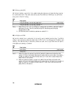
Bits 1 and 0: Clock select 1, 0 (CKS1, CKS0)
Bits 1 and 0 choose ø/64, ø/16, øw/2, or ø as the clock source for the baud rate generator.
For the relation between the clock source, bit rate register setting, and baud rate, see 8, Bit rate
register (BRR).
Bit 1
CKS1
Bit 0
CKS0
Description
0
0
ø clock
(initial value)
0
1
ø w/2 clock
*
1
/ø w clock
*
2
1
0
ø/16 clock
1
1
ø/64 clock
Notes: 1. ø w/2 clock in active (medium-speed/high-speed) mode and sleep mode
2. ø w clock in subactive mode and subsleep mode
3. In subactive or subsleep mode, SCI3 can be operated when CPU clock is øw/2 only.
10.2.6
Serial control register 3 (SCR3)
Bit
Initial value
Read/Write
7
TIE
0
R/W
6
RIE
0
R/W
5
TE
0
R/W
4
RE
0
R/W
3
MPIE
0
R/W
0
CKE0
0
R/W
2
TEIE
0
R/W
1
CKE1
0
R/W
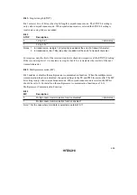
SCR3 is an 8-bit register for selecting transmit or receive operation, the asynchronous mode clock
output, interrupt request enabling or disabling, and the transmit/receive clock source.
SCR3 can be read or written by the CPU at any time.
SCR3 is initialized to H'00 upon reset, and in standby, module standby or watch mode.


