203
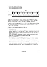
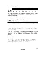
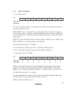
5. Clock stop register 1 (CKSTPR1)
—
TFCKSTP TCCKSTP TACKSTP
S31CKSTP S32CKSTP ADCKSTP TGCKSTP
7
6
5
4
3
2
1
0
1
1
1
1
1
1
1
1
R/W
R/W
R/W
R/W
R/W
R/W
R/W
R/W
Bit:
Initial value:
Read/Write:
CKSTPR1 is an 8-bit read/write register that performs module standby mode control for peripheral
modules. Only the bit relating to timer F is described here. For details of the other bits, see the
sections on the relevant modules.
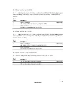
Bit 2: Timer F module standby mode control (TFCKSTP)
Bit 2 controls setting and clearing of module standby mode for timer F.
TFCKSTP
Description
0
Timer F is set to module standby mode
1
Timer F module standby mode is cleared
(initial value)
9.4.3
CPU Interface
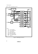
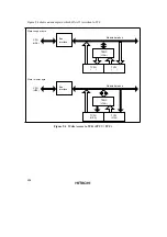
TCF and OCRF are 16-bit read/write registers, but the CPU is connected to the on-chip peripheral
modules by an 8-bit data bus. When the CPU accesses these registers, it therefore uses an 8-bit
temporary register (TEMP).
In 16-bit mode, TCF read/write access and OCRF write access must be performed 16 bits at a time
(using two consecutive byte-size MOV instructions), and the upper byte must be accessed before
the lower byte. Data will not be transferred correctly if only the upper byte or only the lower byte
is accessed.
In 8-bit mode, there are no restrictions on the order of access.
1. Write access
Write access to the upper byte results in transfer of the upper-byte write data to TEMP. Next,
write access to the lower byte results in transfer of the data in TEMP to the upper register byte,
and direct transfer of the lower-byte write data to the lower register byte.


