171
8.11.2
Register Configuration and Descriptions
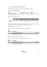
Table 8.27 shows the registers used by the input/output data inversion function.
Table 8.27
Register Configuration
Name
Abbreviation
R/W
Address
Serial port control register
SPCR
R/W
H'FF91
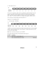
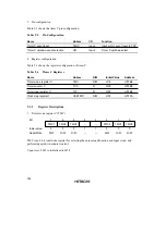
Serial Port Control Register (SPCR)
Bit
Initial value
Read/Write
7
—
1
—
6
—
1
—
5
SPC32
0
R/W
4
SPC31
0
R/W
3
SCINV3
0
R/W
0
SCINV0
0
R/W
2
SCINV2
0
R/W
1
SCINV1
0
R/W
SPCR is an 8-bit readable/writable register that performs RXD
31
, RXD
32
, TXD
31
, and TXD
32
pin
input/output data inversion switching. SPCR is initialized to H'C0 by a reset.
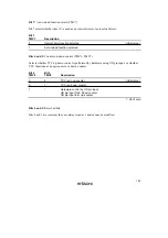
Bit 0: RXD
31
pin input data inversion switch
Bit 0 specifies whether or not RXD
31
pin input data is to be inverted.
Bit 0
SCINV0
Description
0
RXD
31
input data is not inverted
(initial value)
1
RXD
31
input data is inverted
Bit 1: TXD
31
pin output data inversion switch
Bit 1 specifies whether or not TXD
31
pin output data is to be inverted.
Bit 1
SCINV1
Description
0
TXD
31
output data is not inverted
(initial value)
1
TXD
31
output data is inverted


