System Control Coprocessor
ARM DDI 0363E
Copyright © 2009 ARM Limited. All rights reserved.
4-39
ID013010
Non-Confidential, Unrestricted Access
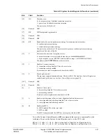
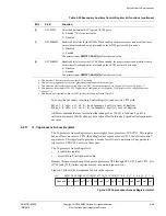
[28]
DIADI
a
Case A dual issue control:
0 = Enabled. This is the reset value.
1 = Disabled.
[27]
B1TCMPCEN
B1TCM parity or ECC check enable:
0 = Disabled
1 = Enabled.
The primary input
PARECCENRAM[2]
b
defines the reset value.
If the BTCM is configured with ECC, you must always set this bit to the same value as
B0TCMPCEN
.
[26]
B0TCMPCEN
B0TCM parity or ECC check enable:
0 = Disabled
1 = Enabled.
The primary input
PARECCENRAM[1]
b
defines the reset value.
If the BTCM is configured with ECC, you must always set this bit to the same value as
B1TCMPCEN
.
[25]
ATCMPCEN
ATCM parity or ECC check enable:
0 = Disabled
1 = Enabled.
The primary input
PARECCENRAM[0]
b
defines the reset value.
[24]
AXISCEN
AXI slave cache RAM access enable:
0 = Disabled. This is the reset value.
1 = Enabled.
Note
When AXI slave cache access is enabled, the caches are disabled and the processor cannot
run any cache maintenance operations. If the processor attempts a cache maintenance
operation, an Undefined instruction exception is taken.
[23]
AXISCUEN
AXI slave cache RAM non-privileged access enable:
0 = Disabled. This is the reset value.
1 = Enabled.
[22]
DILSM
Disable
Low Interrupt Latency
(LIL) on load/store multiples:
0 = Enable LIL on load/store multiples. This is the reset value.
1 = Disable LIL on all load/store multiples.
[21]
DEOLP
Disable end of loop prediction:
0 = Enable loop prediction. This is the reset value.
1 = Disable loop prediction.
[20]
DBHE
Disable
Branch History
(BH) extension:
0 = Enable the extension. This is the reset value.
1 = Disable the extension.
[19]
FRCDIS
Fetch rate control disable:
0 = Normal fetch rate control operation. This is the reset value.
1 = Fetch rate control disabled.
[18]
Reserved
SBZ.
Table 4-24 Auxiliary Control Register bit functions (continued)
Bits
Field Function

